


Content last revised on September 10, 2026
Planar Symmetrical Busbar Geometry: Achieving L_sigma < 20nH to Protect Silicon Junctions
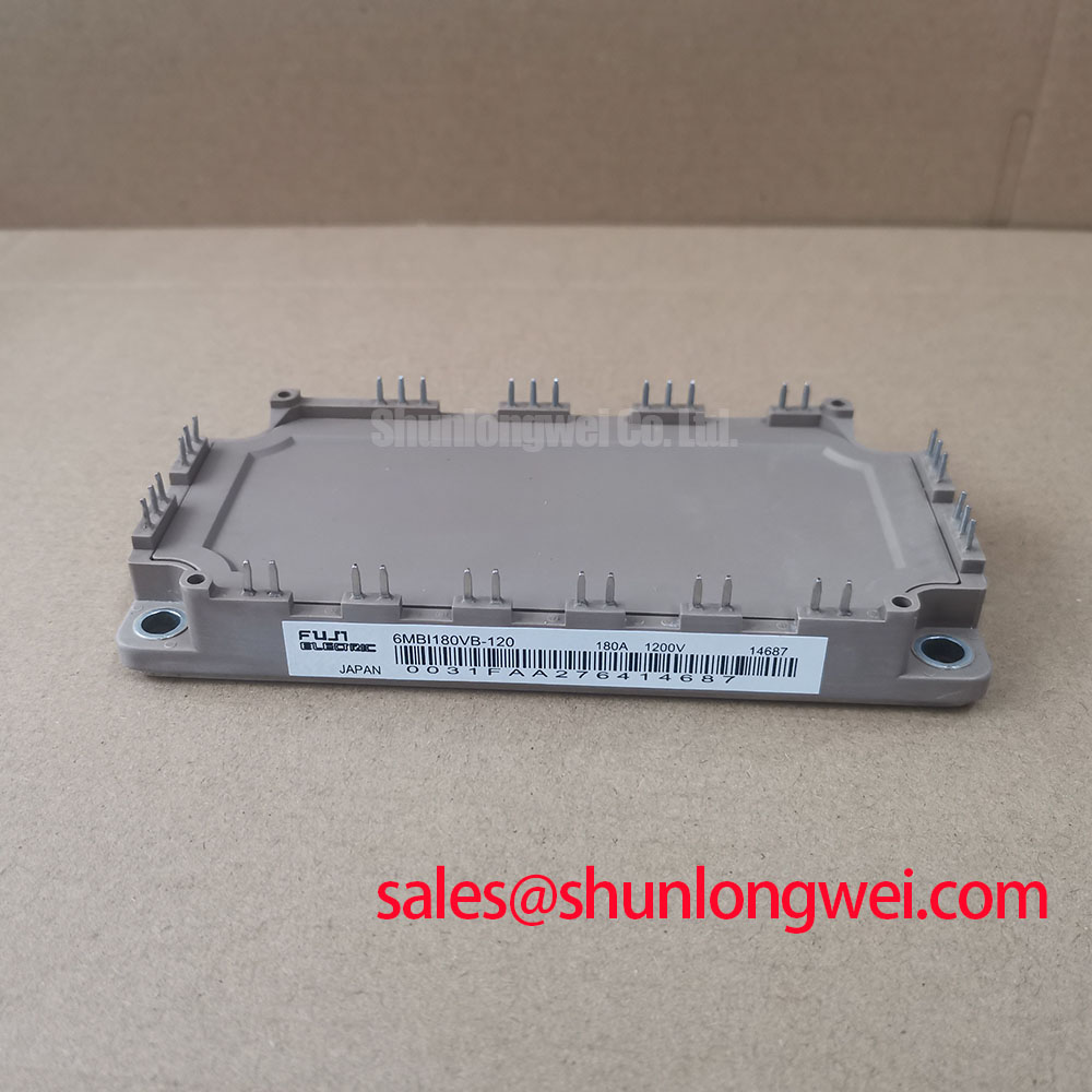
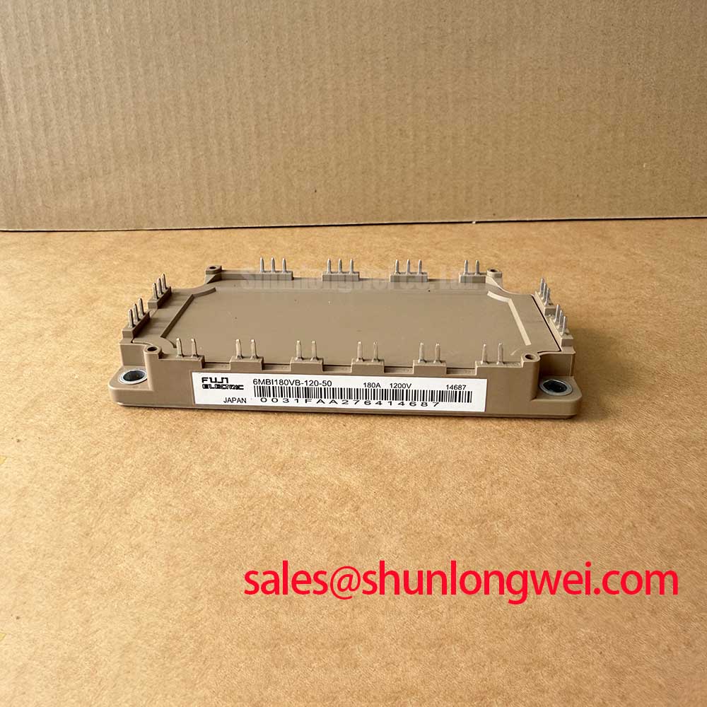
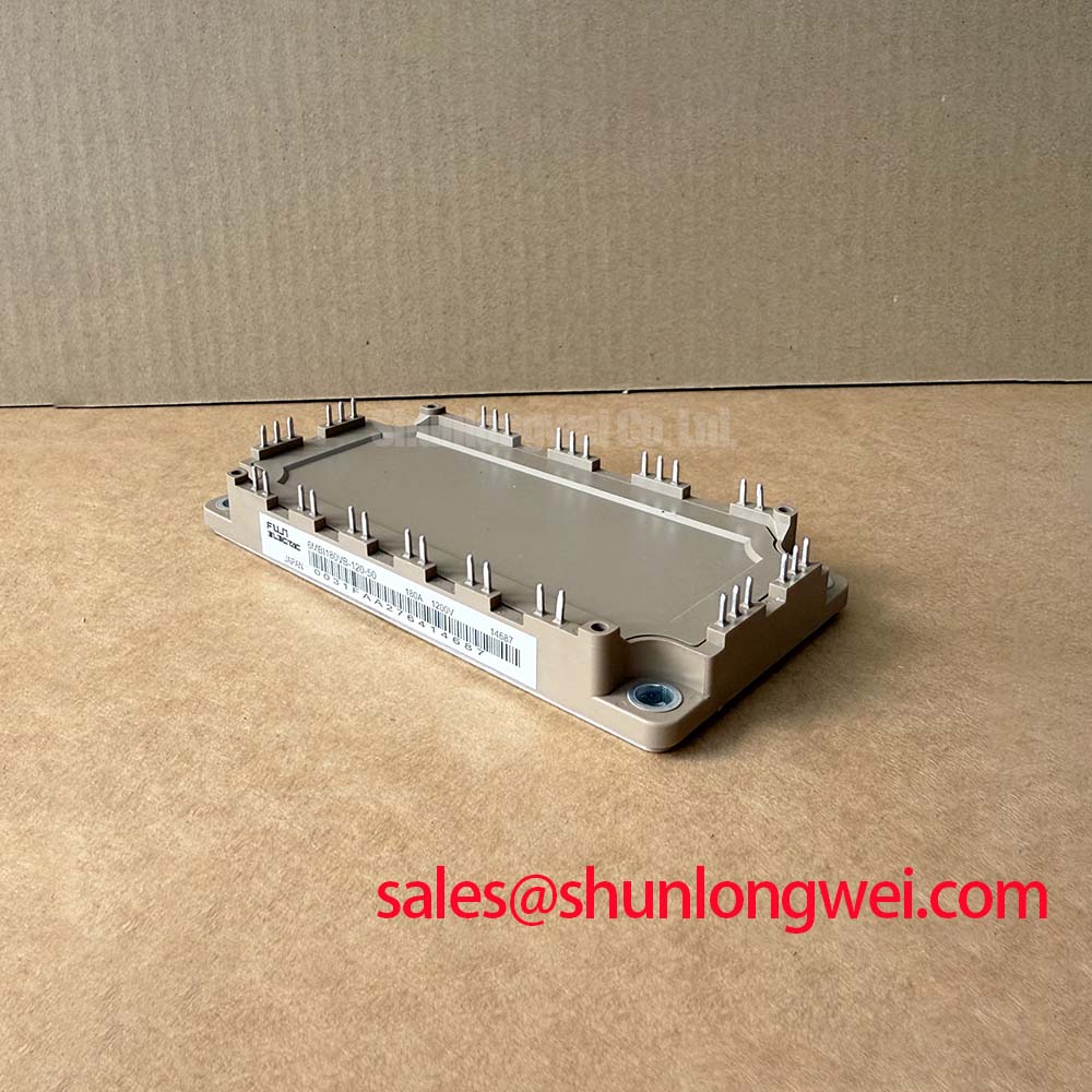
In high-capacity commercial string inverters and micro-grid energy storage systems (BESS), the Fuji Electric 6MBI180VB-120-50 IGBT module operates under demanding power cycling regimes. Rated at a maximum collector-emitter breakdown voltage of VCES = 1200V (Official Datasheet Specification) and a nominal continuous collector current of IC = 150A at Tc = 100°C (180A nominal, with a peak pulse current rating of ICP = 400A for 1ms at Tc = 80°C), managing dynamic voltage overshoot during turn-off transients is vital to prevent catastrophic avalanche breakdown.
When the module interrupts fault currents or undergoes hard switching under full DC-link potential (typically 600V to 850V in 1000V DC commercial PV architectures), the fast turn-off current gradient (di/dt) interacts directly with the total loop parasitic inductance. The total peak turn-off collector-emitter voltage equals the DC-link voltage combined with the dynamic overshoot induced across loop parasitic inductances: Vpeak = VDC + Lσ × (di/dt). If a turn-off event exhibits an instantaneous current ramp of di/dt = 2.5 kA/μs across an unmitigated loop inductance of 60nH, the induced transient spike exceeds 150V, eroding the safe operating area (SOA) margin of the silicon junction.
To restrict parasitic inductance to Lσ < 20nH, engineers must implement laminated, planar symmetrical busbar structures directly over the module power terminals. Running positive and negative DC busplates with minimal inter-plane clearance (0.5 mm to 1.0 mm using high-dielectric-strength Nomex or Kapton film) maximizes magnetic flux cancellation. Placing low-inductance polypropylene film snubber capacitors immediately adjacent to the DC terminal studs creates a localized high-frequency bypass loop. When scaling designs to higher utility-scale current classes, the system topology may transition to higher-capacity packages such as the 6MBI450V-170, where busbar geometry and flux cancellation become even more critical for preserving SOA margins.
The baseline physical parameters for the 6MBI180VB-120-50 are summarized below for rapid hardware benchmarking:
| Parameter | Symbol | Datasheet Rating / Unit | Test Conditions / Definition |
|---|---|---|---|
| Collector-Emitter Voltage | VCES | 1200 V | Tc = 25°C (Official Datasheet Specification) |
| Continuous Collector Current | IC | 150 A (Nominal 180A) | Tc = 100°C (Official Datasheet Specification) |
| Repetitive Peak Pulse Current | ICP | 400 A | 1ms pulse width, Tc = 80°C |
| Collector Saturation Voltage | VCE(sat) | 1.85 V (Chip) / 2.85 V (Terminal) | VGE = 15V, IC = 200A, Tj = 25°C |
| IGBT Thermal Resistance | Rth(j-c) | 0.18 °C/W | Per IGBT device, junction-to-case |
| Isolation Voltage | Viso | 2500 VAC | AC 50/60 Hz, 1 minute test duration |
Baseplate Convexity Compensation and Screw Tightening Sequence Guidelines
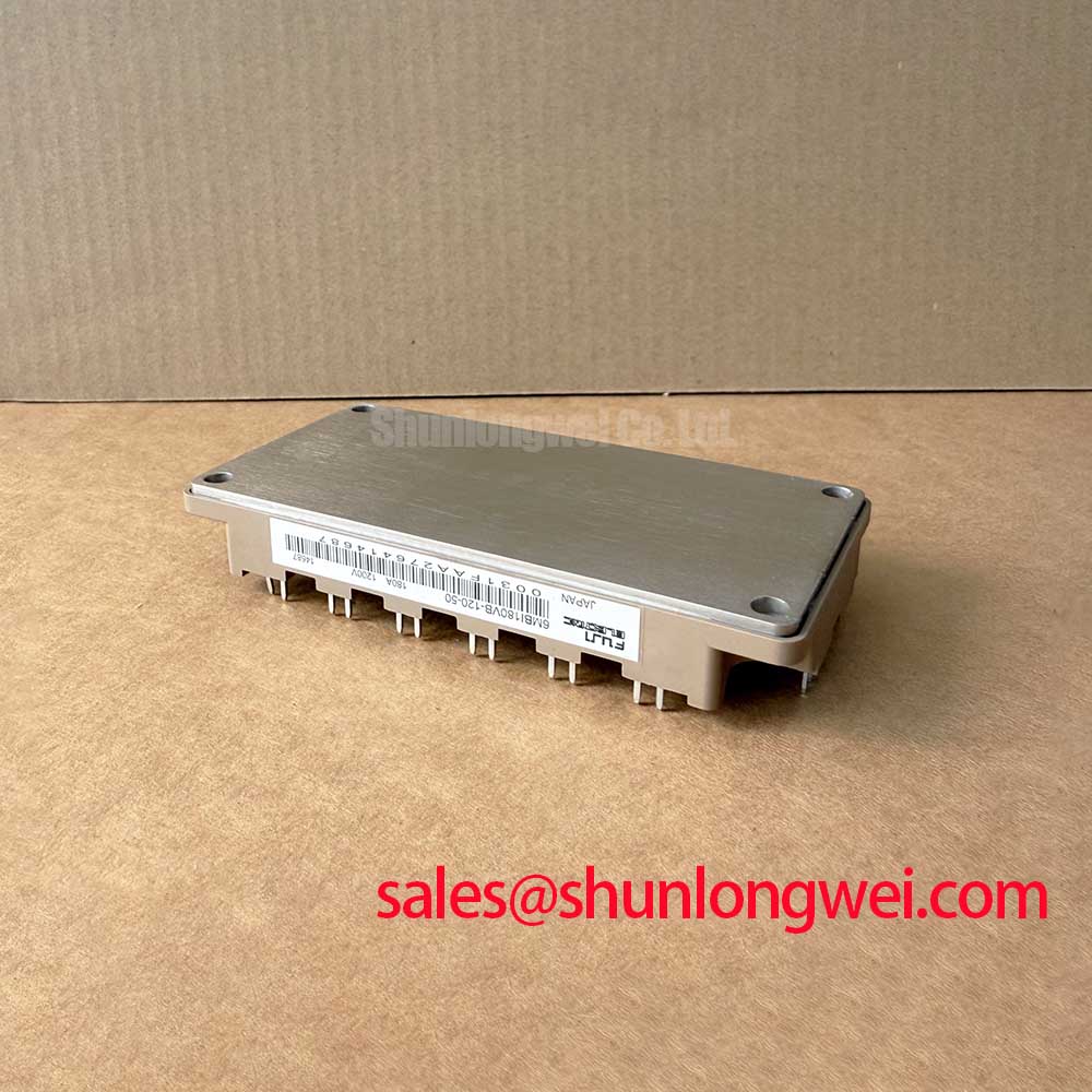
Industrial power modules feature a copper baseplate engineered with a slight pre-bowed convexity. This intentional curvature ensures that when the module is torqued onto a flat heatsink, mechanical pressure forces the thermal interface material (TIM) outward from the center, preventing air entrapment under the IGBT and freewheeling diode (FWD) chips. Improper mounting sequence or excessive torque distorts this profile, causing high localized thermal bottlenecks or cracking the internal Direct Bonded Copper (DBC) ceramic substrate.
Thermal paste application requires a uniform wet thickness between 50μm and 100μm, applied via a precision stainless-steel mesh stencil. Excessively thick paste increases thermal resistance, whereas insufficient grease creates dry voids. Heatsink flatness across the mounting footprint must stay within 50μm per 100mm, with a surface roughness of Rz ≤ 10μm.
💡 Pro Tip: Always use a calibrated, cross-pattern, two-step fastening sequence. For standard M5 mounting screws, apply an initial seating torque of 0.5 N·m to 1.0 N·m across all positions in an "X" sequence (1-4-2-3), then wait 5 minutes to permit the thermal compound to relax and spread laterally. Conclude with the final design torque of 2.5 N·m to 3.5 N·m (General Industry Design Consideration for M5 module mounting). Never torque one corner to full rating while adjacent fasteners remain loose, as this creates asymmetrical shear stress on the internal ceramic isolation layer.
Fast-recovery diodes operating in hard-switched inverter topologies can exhibit high-frequency ringing if the baseplate is inadequately grounded or if reverse recovery current (Irr) snappy transitions couple into the heatsink chassis. Proper baseplate bonding ensures both thermal dissipation and minimal radiated EMI emission across industrial switching bands, matching benchmarks described in foundational power electronics literature and resources such as Fuji Electric Discrete IGBT & SiC MOSFETs technical documentation.
Transient Thermal Impedance (Zth(j-c)) & Multi-Layer Foster/Cauer Modeling
Commercial inverters and micro-grid storage converters regularly encounter short-term transient overloads, such as motor-starting inrush currents or grid-frequency stabilization pulses. Under these dynamic conditions, steady-state thermal resistance (Rth(j-c) = 0.18 °C/W for the IGBT section) is insufficient to predict silicon junction temperatures (Tj). Engineers must utilize the transient thermal impedance curve, Zth(j-c)(t), modeled via multi-element Foster or Cauer RC networks.
The silicon chip responds nearly instantaneously to pulse widths under 1 ms, where thermal energy remains concentrated within the silicon die volume (governed by the first thermal RC time constant, typically τ1 ≈ 1 ms to 10 ms). For pulses between 10 ms and 1 second, heat spreads through the solder layer into the copper baseplate (τ2 ≈ 50 ms to 200 ms). Pulses exceeding several seconds engage the thermal mass of the external heatsink.
When running overload cycles during peak power injection, calculate the peak junction temperature margin against the absolute maximum limit of Tj(max) = 150°C. For continuous operation, maintaining Tj(op) ≤ 125°C is a recommended design guideline to protect the bond wires and solder interfaces from thermal fatigue. If unexpected over-temperature trips occur during field commissioning, verify the dynamic heatsink thermal path against standard troubleshooting protocols detailed in the Field Engineer’s Handbook.
Kelvin Emitter Connection & Parasitic Inductance Minimization in High-Speed Switching
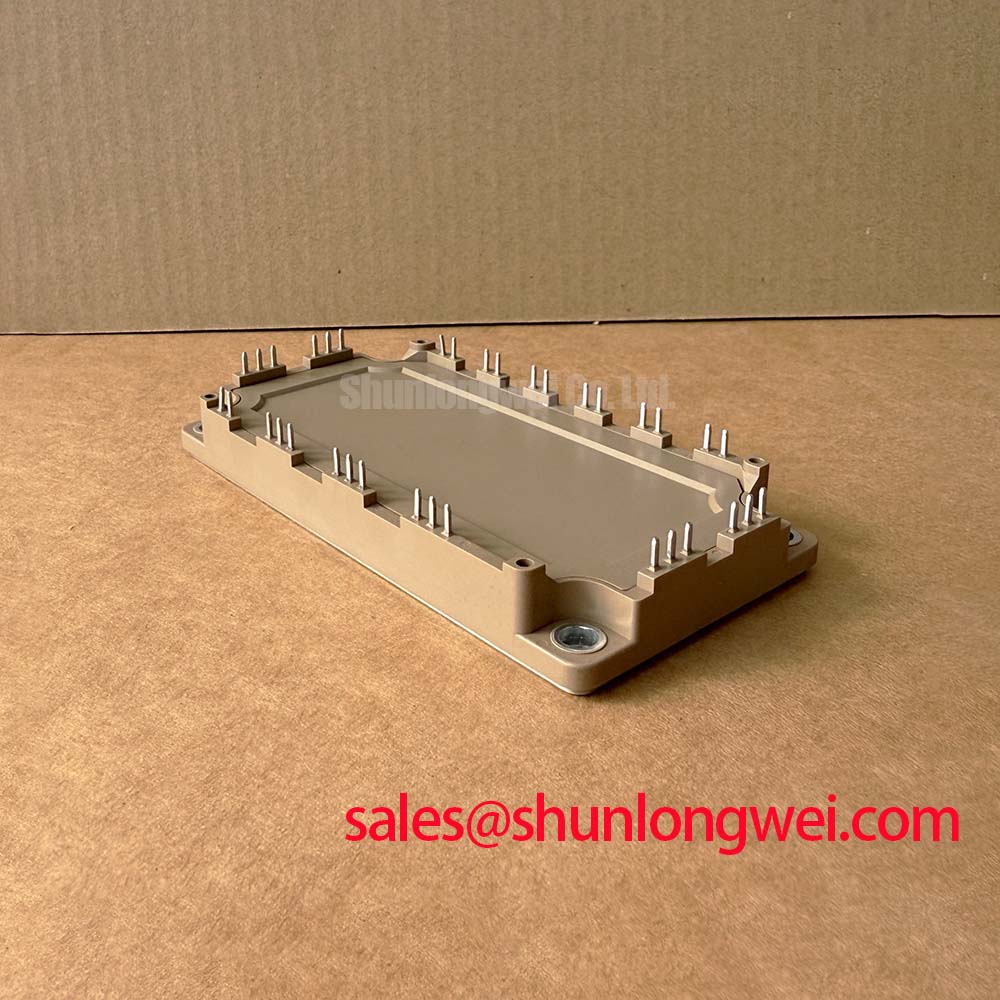
The 6MBI180VB-120-50 incorporates auxiliary Kelvin emitter terminals alongside the primary high-current power terminals. In high-speed switching operations, high di/dt passing through the main emitter loop induces an opposing voltage across any shared stray inductance (Le). This induced voltage acts as negative dynamic gate feedback, slowing down gate charging, increasing switching losses (Eon and Eoff), and potentially triggering parasitic Miller-induced oscillations.
By routing the gate driver's return reference directly to the auxiliary Kelvin emitter terminal, the gate drive charging loop is decoupled from the main load path. To preserve this isolation integrity on the PCB layout:
- Route the gate and Kelvin emitter tracks as closely coupled differential pairs directly from the isolated gate driver IC output pins to the module terminals.
- Maintain a gate loop area under 2 cm² to minimize susceptibility to radiated electromagnetic interference generated by adjacent phase legs.
- Place the gate resistor (typical starting value RG = 4.7 Ω to 15 Ω) as close as physically possible to the module's gate terminal.
- Implement an active Miller clamp or provide a negative turn-off bias (e.g., -5V to -8V) to ensure the gate-emitter voltage stays firmly below the conduction threshold during high dv/dt transitions of the complementary switch.
When diagnostic checks or field servicing require validation of digital control inputs and driver interconnect integrity, digital boundary scan methodologies like the Boundary Scan (JTAG IEEE 1149.1) Digital Test Protocol allow direct verification of driver board continuity before applying high-voltage DC power to the main bus.