Content last revised on September 28, 2026
Preventing Spurious Faults: Negative Gate Bias vs Active Miller Clamp Guidelines for MIG75Q201H
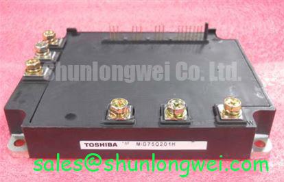
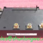
With the DC link discharged and isolated, compare the cold terminal-to-terminal readings of the MIG75Q201H against the equipment schematic before connecting a gate driver. Toshiba identifies this device as an IGBT module with a rated voltage of 1200 V and rated current of 75 A (Official Specifications). Those ratings establish identification boundaries, not permission to apply the full values at every switching frequency, case temperature, or cooling condition. A repair assessment should also confirm the terminal arrangement, mounting interface, and original circuit function against the documentation for the installed assembly.
A drive that reports intermittent gate faults after module replacement deserves a measurement at the gate terminals, not an immediate change to the driver settings. During switching in a complementary leg, rapid collector-voltage movement can couple through an IGBT’s gate-to-collector capacitance and lift the gate of the device intended to remain off. If that lift reaches a turn-on condition, unwanted conduction becomes possible. This is a general switching mechanism (Design Consideration), not a documented fault characteristic of the MIG75Q201H.
Negative off-state bias and an active Miller clamp are different ways for a system designer to control that risk. Negative bias increases separation between the off-state gate voltage and the turn-on threshold; a clamp provides a low-impedance path near the gate while the device is off. Neither establishes a suitable driver configuration by itself. The integrator should check the installed driver’s permitted gate-voltage range, clamp connection, fault response, and the module’s applicable gate limits in the original Toshiba documentation before changing either approach. No off-state bias value or clamp performance threshold can be inferred from the module’s 1200 V and 75 A ratings.
Keep the gate-drive loop physically distinct from the high-current switching path where the confirmed terminal arrangement allows it. Short, closely coupled gate and return conductors help limit induced voltage; routing them alongside a collector bus or through a shared power return can obscure what voltage the gate actually sees. On a suspected high-dv/dt fault, capture gate-to-emitter voltage at the module connection during both turn-on and turn-off, then correlate each disturbance with the opposing switch transition. Measurements at the driver board alone can miss voltage developed across the interconnecting conductors.
Turn-off overshoot needs its own check. Busbar geometry, loop inductance, current, and switching behavior affect the peak collector voltage, so the designer should verify the measured peak against the module rating under representative operating conditions. A snubber network is one possible system-level means of managing a switching transient, but its components and placement require circuit-specific testing rather than selection from the module voltage rating alone. 💡 Pro Tip: Keep opposing busbar current paths closely paired to reduce turn-off loop inductance, then verify the resulting voltage margin with switching measurements.
MIG75Q201H Operational Boundaries: Evaluating Kelvin Emitter Connection Limits
Before assigning a separate emitter return on the MIG75Q201H, identify its terminals from the original module drawing. The supplied product ratings do not establish that this unit has an auxiliary Kelvin emitter connection. Treating an unverified terminal as a driver return risks an incorrect connection, and describing Kelvin routing as an inherent feature would overstate the available specification.
If the documented terminal arrangement provides a dedicated auxiliary emitter, the driver return should be assessed separately from the main current-carrying emitter path (Design Consideration). Power-current changes create voltage across shared conductor impedance. That voltage can appear in series with the commanded gate signal, contributing to apparent gate bounce or oscillation. Separating the sensing return from the power path addresses the coupling mechanism; it does not eliminate the need to inspect the complete gate loop, connector condition, and driver output waveform. If no auxiliary emitter is documented, the engineer must work from the actual terminal map and measure the effect of the available return path.
Complementary switch timing also belongs to the drive controller and gate-driver design, not to a presumed feature of this module. An interlock should prevent simultaneous gate commands, while the required dead time must be established using the documented switching behavior and measured waveforms across the operating envelope (Design Consideration). Excessive dead time can affect output waveform quality; insufficient dead time can permit overlap after accounting for propagation delays and turn-off behavior. During commissioning, compare both gate signals at the module connections and inspect the driver’s fault history before attributing an overcurrent event to a single component.
For a potential heavy-duty variable frequency AC motor drive repair, compare the installed assembly and any proposed replacement on topology, terminal assignment, driver compatibility, thermal interface, and documented operating conditions. The MG75H6EL1 can be included in a sourcing comparison, but its model designation alone does not establish electrical or mechanical interchangeability with the MIG75Q201H. Where the drive uses a phase-controlled input rectifier, its firing-angle behavior and resulting line harmonics should be assessed at the equipment level; neither is an intrinsic specification of the IGBT module.
Field Diagnostics and Commissioning: Braking Resistors and Chopper Transistors in MIG75Q201H Topologies
Trace the actual DC-link and braking circuit before assigning a braking role to the MIG75Q201H. The supplied specifications identify an IGBT module but do not establish that it contains a braking transistor, a particular number of switches, or an integrated resistor. A drive may place those functions elsewhere. The wiring diagram and module terminal map determine whether this device participates in inverter switching, braking, or another stage.
In a drive that uses a brake chopper, motor deceleration can return energy to the DC link. The chopper and resistor must be assessed against the machine’s operating cycle, allowable DC-link excursion, resistor thermal limits, and the documented limits of the switching device (Design Consideration). A resistor chosen only by its nominal resistance may not withstand repeated braking pulses; a transistor judged only by continuous current may not have adequate margin for the actual pulse and cooling conditions. The system engineer should establish those requirements from the equipment design and validate them during controlled commissioning rather than treating the module’s 75 A rating as a brake-sizing instruction.
If a drive trips during deceleration, record DC-link voltage, brake command, chopper gate waveform, and relevant fault codes on the same time base. An elevated DC link may be consistent with ineffective energy dissipation, but it does not by itself distinguish a control problem, open resistor path, wiring issue, or switching-device fault. With power safely isolated, resistance and continuity checks can narrow the investigation; live waveform tests then establish whether the commanded action reaches the installed transistor. Disconnect and discharge the DC link before moving measurement leads or removing braking-circuit connections.
Motor-cable effects should be kept separate from a brake-circuit diagnosis. A long cable can produce reflected-wave voltage at the motor terminals, depending on cable characteristics and pulse rise time; that measurement is not the same as collector-voltage overshoot at the module. If the equipment uses an output filter, assess its suitability from measured motor-terminal waveforms and the drive documentation. For repeatable test notes and fault isolation, the Field Engineer’s Handbook provides a practical companion to the equipment-specific procedures.
MIG75Q201H Circuit Protection and Reliability: Checking Isolation and Driver Behavior
Do not infer a reinforced isolation rating, barrier test voltage, or common-mode transient immunity rating from the MIG75Q201H part number. The supplied module specifications establish 1200 V, 75 A, and a module package; they do not specify the isolation performance of an associated gate-driver supply or signal isolator. Those properties belong to the identified components and to the finished equipment’s insulation design. The integrator should consult the applicable manufacturer documents and equipment safety file before describing any barrier as reinforced.
When investigating unexpected gate pulses, inspect the gate-driver supply and isolated command path alongside the module waveform. Compare the command entering the driver with its output at the module while the power stage operates under controlled conditions. A pulse appearing only at the output warrants examination of local supply stability, layout coupling, and the driver’s documented common-mode behavior; a pulse present at the input directs attention upstream. The required immunity and insulation spacing depend on the equipment architecture and verified operating transients (Design Consideration), not a universal value assigned to this module.
Isolation language also needs precision at service interfaces. SELV and PELV describe electrical safety arrangements under defined system conditions; neither label follows automatically from installing an IGBT or an isolated driver. Creepage, clearance, protective bonding, enclosure access, and test method should be checked against the requirements applicable to the completed equipment. Avoid applying an insulation test to connected electronics until the equipment procedure identifies which assemblies must be disconnected.
For thermal assessment, record the cooling condition and load profile rather than assuming that the 75 A rating describes every pulse. Junction-temperature estimates for repeated or short-duration loading require the relevant manufacturer thermal data, including transient thermal impedance where available, plus a defensible estimate of conduction and switching losses (Engineering Calculation). Without those inputs, a numerical junction-temperature margin would be speculative. Finish commissioning by recording measured DC-link peaks, module gate waveforms, fault response, and cooling conditions at the operating points the equipment must actually withstand.