Content last revised on September 15, 2026
MG30J103H Electrical Profile for Servo Drive Evaluation
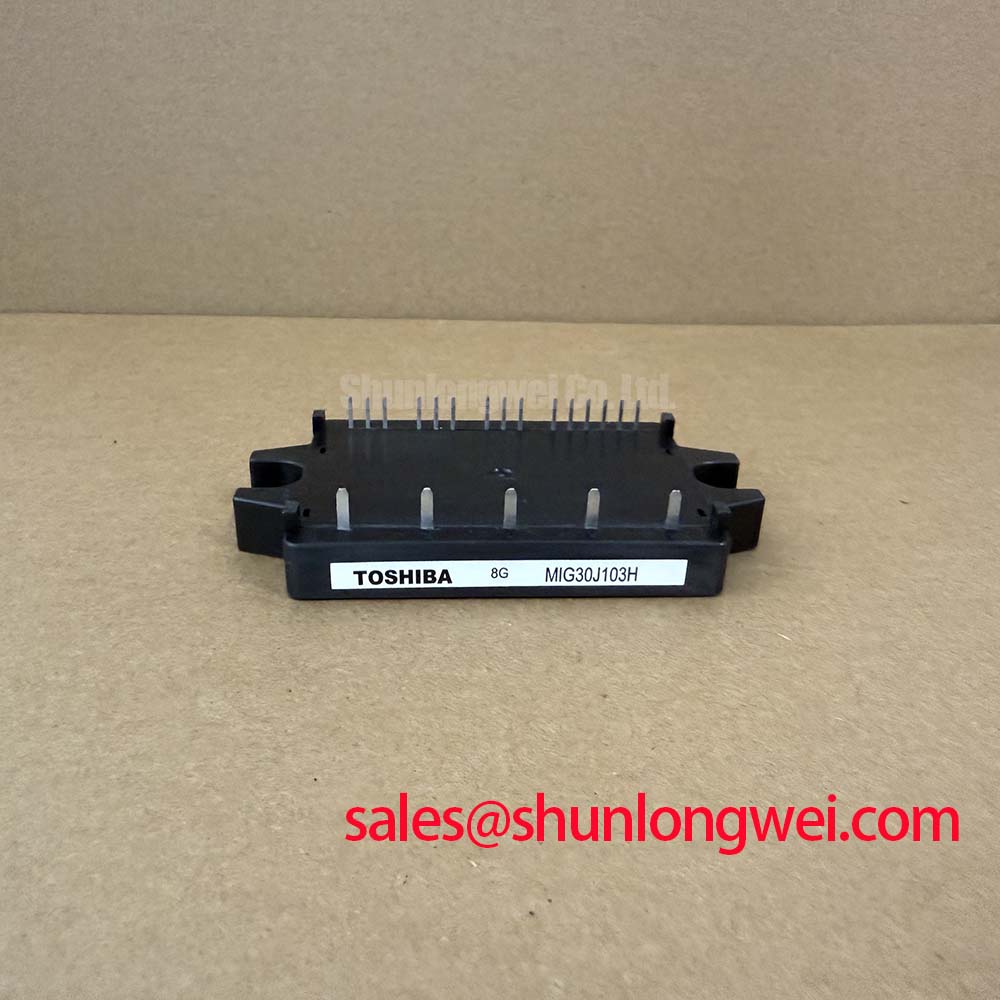
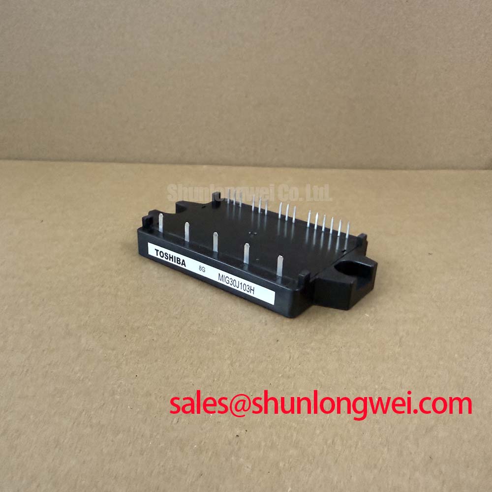
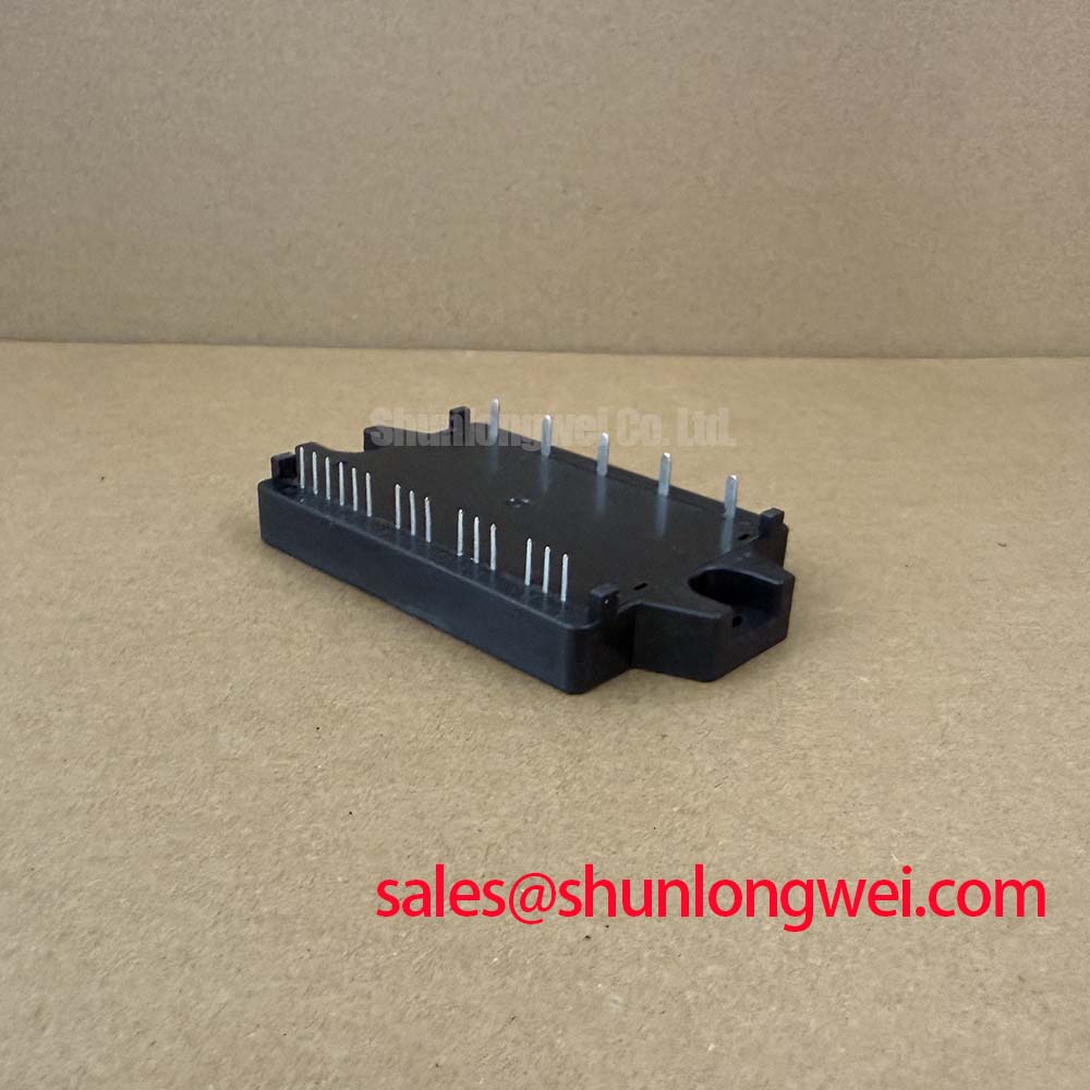
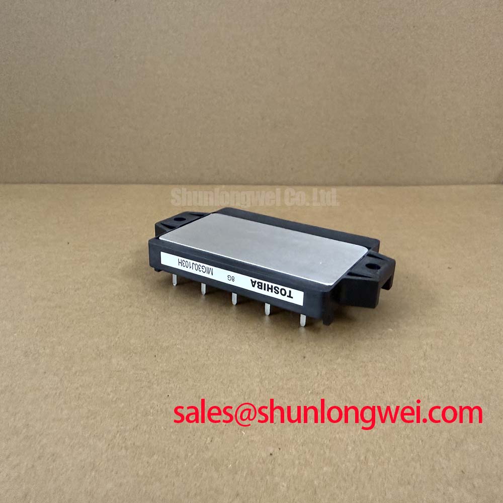
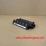
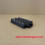
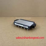
Begin a replacement inspection with power isolated: verify the marking on the Toshiba MG30J103H, check the module body for mechanical damage, and compare the original drive’s DC link rating with the module’s published electrical boundary. The supplied official specification identifies this device as a Toshiba IGBT module with a 600 V VCES collector emitter voltage rating and a 30 A IC rated collector current.
The published maximum collector emitter saturation voltage is 2.7 V VCE(sat). This value belongs to the manufacturer’s specified test conditions, so a service engineer should not treat it as a universal operating voltage under every switching current, junction temperature, or gate drive condition. Actual dissipation must be checked against the switching frequency, conduction profile, cooling path, and measured case temperature.
| Parameter | Official Specification |
| Collector emitter voltage | 600 V VCES |
| DC collector current | 30 A IC |
| Maximum collector emitter saturation voltage | 2.7 V VCE(sat) |
| Collector power dissipation at Tc = 25°C | 83 W PC |
| Control supply voltage | 20 V VD |
| Fault output voltage | 20 V VFO |
| Fault output current | 7 mA IFO |
| Isolation voltage for one minute AC test | 2500 Vrms VISO |
| Typical module weight | 80 g |
The official data supplied for this product does not specify an ITSM surge current limit, an I²t short circuit withstand value, a junction temperature recovery window, or a complete switching loss map. Those values should be obtained from the applicable Toshiba documentation or validated on the target inverter rather than estimated from the 30 A DC rating. A semiconductor fast fuse and the module’s short circuit protection must therefore be coordinated from verified time current and energy data.
For a high dynamics multi axis CNC or robotics servo, designers should compare the original gate driver, fault interface, DC link, braking circuit, and cooling assembly before approving a replacement. The MG100Q1ZS40 may be reviewed as a separate Toshiba module reference, but electrical compatibility must be established from its own documentation and the machine schematic.
Planar Busbar Geometry and Spurious Fault Investigation
Inspect the commutation loop before changing protection components. A wide, closely coupled positive and negative DC bus path generally reduces stray inductance, while long separated conductors increase switching overshoot and radiated noise. During turn off, the additional voltage created by loop inductance and current change adds to the DC link voltage; the resulting peak must be captured at the module terminals with a properly rated differential probe.
This is a Design Consideration, not an MG30J103H factory limit: keep the high current forward and return paths physically close, maintain consistent phase leg geometry, and prevent control wiring from running parallel to the switching loop. The required creepage and clearance are system determined by working voltage, pollution environment, insulation system, and applicable safety standard. A busbar arrangement that appears symmetrical mechanically still needs oscilloscope confirmation at the actual module terminals.
Snubbers should be selected from measured ringing energy and switching waveforms rather than copied from another inverter. An RC network can reduce high frequency voltage oscillation, but its resistor pulse capability, capacitor dielectric behavior, thermal loss, and impact on turn off energy require verification. If a fault appears only at high load, compare collector emitter voltage, gate emitter voltage, phase current, and fault output timing on a known good operating sequence.
The supplied official specification lists PC = 83 W at Tc = 25°C, but that figure is not a complete thermal design prescription. Heatsink resistance, interface condition, airflow, switching loss, and case temperature measurement determine whether the module remains within its permitted junction conditions. The module’s 2500 Vrms isolation rating for a one minute AC test should also be interpreted within the complete mechanical insulation structure, not as permission to ignore the drive’s system insulation design.
Common Mode Bearing Current and Motor Cable Effects
Long motor leads can behave as a transmission path rather than an ideal connection. Reflections caused by cable impedance, motor terminal impedance, connector geometry, and switching edge content can raise terminal voltage and increase common mode current. A high frequency bearing current symptom should therefore be investigated across the inverter, cable shield termination, motor frame bonding, shaft grounding arrangement, and bearing condition instead of being assigned to the IGBT module alone.
A Design Consideration for CNC and robot servo integration is to evaluate the output filter and common mode choke as a complete network. The chosen filter must support the phase current and fundamental frequency while controlling switching energy, voltage drop, resonance, and thermal rise. Phase angle conduction and line frequency ripple smoothing belong to the rectifier and DC link design; they should be checked with the actual mains impedance and load profile.
RC suppression at the switching node may help control a narrow ringing band, but it can also increase turn off loss. Measure the waveform at the module pins and at the motor terminals, then compare the two locations. If the disturbance grows along the cable, investigate impedance mismatch and termination strategy. If it is already present at the module, review busbar layout, local decoupling, snubber placement, and gate drive timing.
Fault reporting also needs careful interpretation. The official values are VFO = 20 V and IFO = 7 mA. The control board should verify how this output is pulled up, isolated, filtered, and interpreted, because the external interface determines the actual logic waveform. Do not connect the fault output solely by matching voltage labels; confirm polarity, reference potential, and protection behavior against the original circuit documentation.
Gate Drive Loop Geometry for Commissioning
During commissioning, probe the gate emitter voltage directly at the module terminals and keep the probe loop short. The power emitter path carries substantial switching current, so shared copper between the gate return and the main emitter path can introduce mutual coupling into the gate signal. This may appear as ringing, false turn on, irregular fault timing, or inconsistent current sharing between phases, but each symptom requires waveform correlation rather than a single assumed cause.
An Engineering Recommendation is to route the gate drive supply and return as a compact pair, separate the auxiliary control return from the high current emitter path where the module interface permits it, and place the driver’s local bypass components close to the gate connection. The final loop geometry is system determined by the driver output stage, isolation arrangement, switching speed, and board construction. Verify the result during double pulse and loaded switching tests while observing gate voltage, collector emitter voltage, and phase current together.
The Miller plateau is influenced by the effective transfer capacitance, switching voltage slope, driver impedance, and external circuit inductance. Because the supplied official parameter list does not provide a complete Cres or gate charge switching table, designers should obtain the correct Toshiba test data before calculating a gate resistor or clamp response. A bench adjustment should be treated as a Typical Starting Point only, followed by thermal and transient validation at the real DC link and motor load.
Pro Tip: Remove control connectors only after the DC link has been discharged and the absence of hazardous voltage has been verified.
Negative Gate Bias and Active Miller Clamp Selection
High dv/dt can couple energy through the effective gate collector capacitance of an adjacent device. A negative off bias can increase the margin against unintended gate voltage rise, while an active Miller clamp provides a low impedance path during the vulnerable turn off interval. These are Design Considerations rather than published MG30J103H requirements; the appropriate method depends on the isolated driver, gate insulation, fault response, and measured gate waveform.
Do not impose a negative gate voltage from a generic assumption. The supplied official information identifies a 20 V VD control supply rating, but it does not define a permitted negative gate bias range. The system integrator should verify the gate emitter voltage limits, driver common mode behavior, startup sequence, shutdown sequence, and clamp current from the applicable Toshiba and gate driver documentation.
Active Miller clamping should be placed with a low impedance connection to the gate return and coordinated with dead time, desaturation or overcurrent detection, and fault output handling. If cross conduction is suspected, capture both devices’ gate emitter voltages and collector emitter transitions at the same time. Check whether the event follows a control timing command, a busbar transient, a motor cable reflection, or an unstable isolated supply.
For lifetime assessment, avoid converting one measured temperature into a guaranteed service duration. The Arrhenius equation is a modeling framework that requires validated activation energy, temperature profile, failure mechanism, and test evidence. It is not a substitute for Toshiba reliability data. For equipment that combines the servo inverter with an operator display, optical glare control is a separate system issue; the principles of anti reflective coating should not be confused with the electrical protection of the IGBT stage.
Extended evaluation can also reference the Evolution of Negative Off Bias Gate Drive Circuits for general circuit principles. Final approval remains dependent on measured switching margins, insulation tests, thermal behavior, fault timing, and the original CNC or robotics servo system requirements.