Content last revised on September 19, 2026
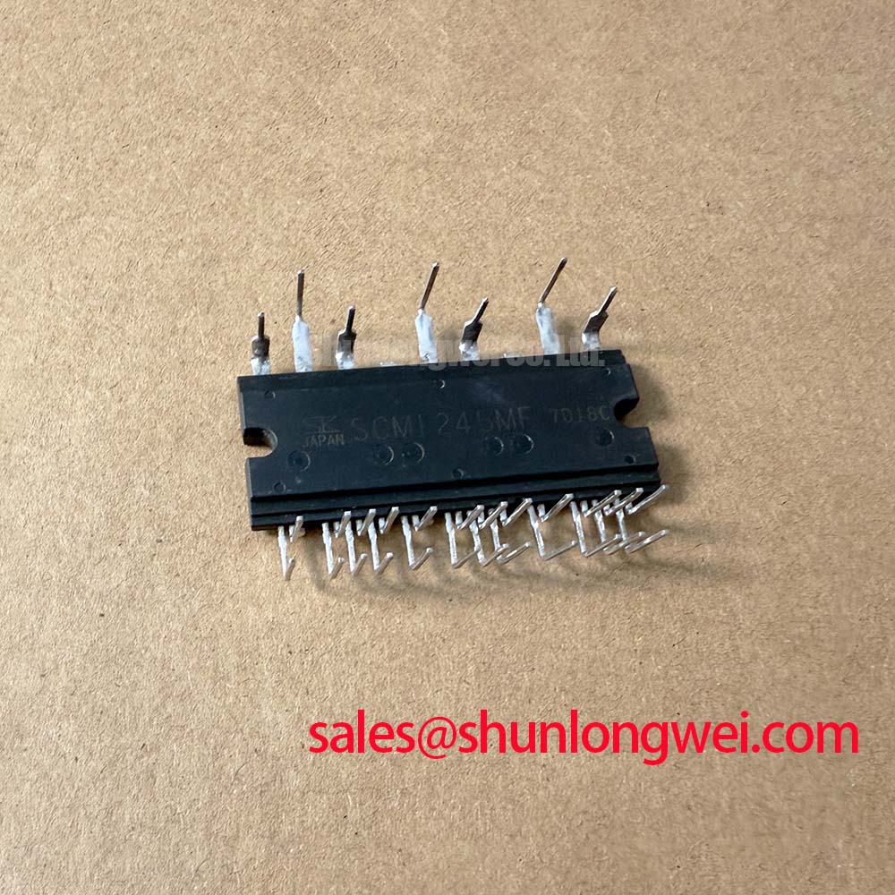
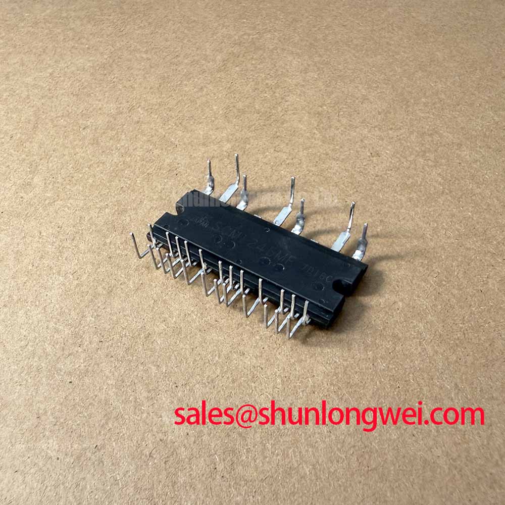
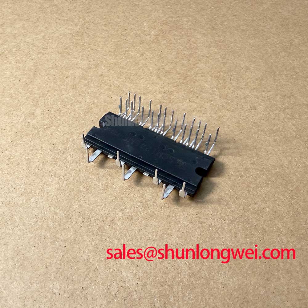
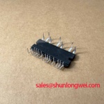
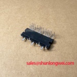
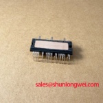
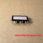
SCM1245MF Sanken 600 V 15 A IGBT Module
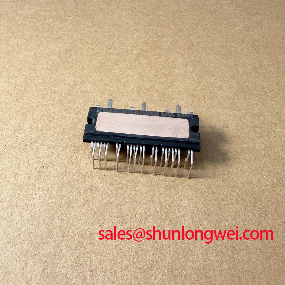
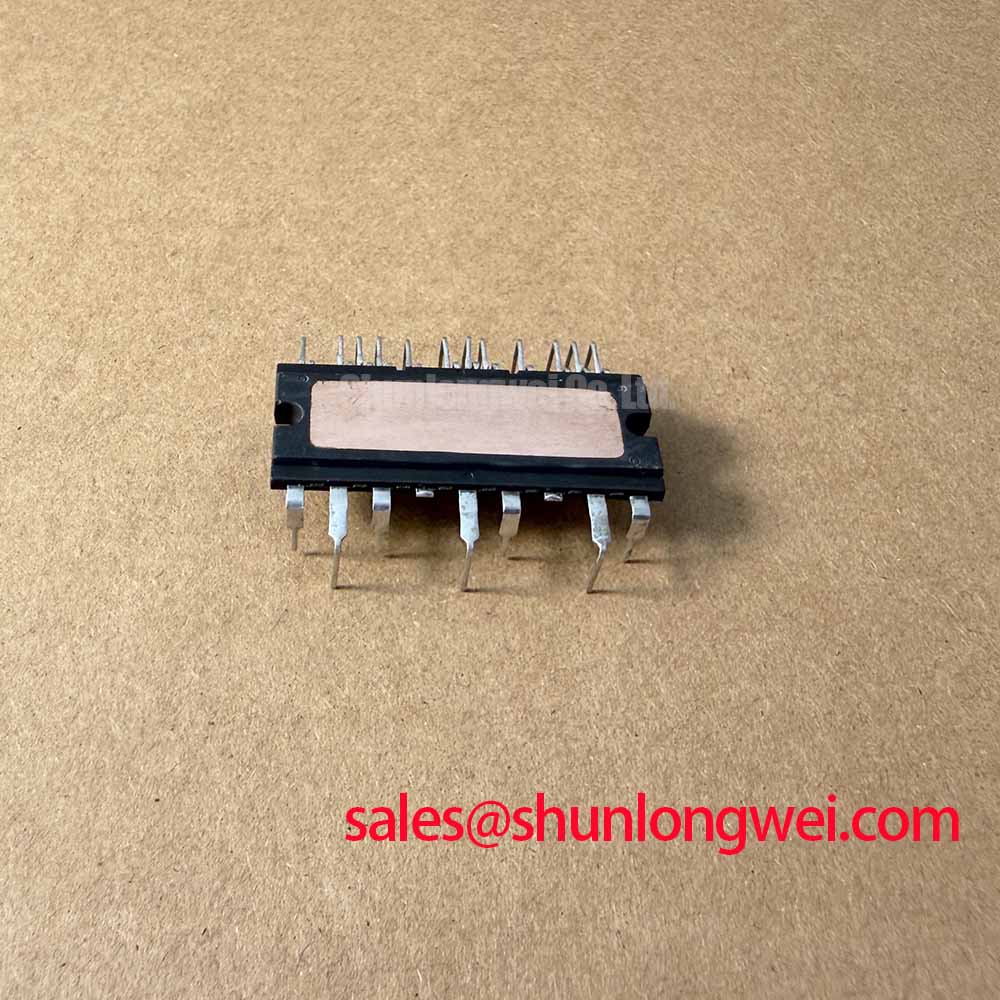
Begin a service evaluation by confirming the SCM1245MF marking, checking the DIP33 package for visible cracks or deformation, and verifying the converter nameplate against the module’s electrical limits before applying power. The Sanken SCM1245MF is an IGBT module specified for a 600 V collector emitter voltage, 15 A rated collector current, and 30 A peak collector current. Its stated isolation voltage is 2500 Vrms, while the specified supply voltage is 15 V.
These values are official product specifications and should be treated as the starting boundary for circuit review. They do not, by themselves, establish an allowable operating point for every inverter topology, switching frequency, ambient condition, or cooling arrangement. The system engineer should verify the original application documentation, gate driver requirements, thermal path, protection timing, and measured switching waveforms before approving a replacement or repair.
| Parameter | Symbol | Value | Unit |
|---|---|---|---|
| Collector Emitter Voltage | Vces | 600 | V |
| Rated Collector Current | Ic | 15 | A |
| Peak Collector Current | Icp | 30 | A |
| Supply Voltage | Vcc | 15 | V |
| Isolation Voltage | Viso | 2500 | Vrms |
| Package Type | Package | DIP33 | Not applicable |
For a commercial string inverter or micro grid energy storage service board, the module should be assessed as part of the complete switching leg. Confirm the DC link voltage, phase current, freewheel path, gate driver supply, isolation arrangement, current sensing, and short circuit response as one system. A compatible device such as 6MBI15L 060 may also be reviewed during material substitution work, but the engineer must compare its complete datasheet and terminal arrangement with the original assembly before making a change.
Preventing Spurious Faults: Thermal Time Constants and Peak Junction Guidelines for SCM1245MF
When a repaired inverter shows intermittent overcurrent or thermal alarms, record the electrical and thermal conditions during the event rather than assigning the fault to the IGBT module alone. The rated collector current specification of 15 A and peak collector current specification of 30 A are official ratings, but the usable current in a real assembly depends on case temperature, heat sink performance, switching losses, pulse duration, duty cycle, and the thermal impedance of the installed structure.
A practical thermal review should begin with the measured case temperature near the module mounting area and the actual current waveform at the collector path. Short overload pulses can produce a junction temperature rise before the case or heat sink responds. Engineers can represent this behavior with a transient thermal impedance network using several RC time constants, provided that the network values come from the applicable Sanken technical documentation or a validated thermal model. The peak junction estimate should then be compared with the manufacturer’s permitted junction conditions, not with an assumed generic semiconductor limit.
For field troubleshooting, compare a known good phase leg with the suspect leg under the same DC link and load conditions. Check whether current sharing changes during turn on, turn off, or freewheel commutation. An abnormal difference may involve gate loop inductance, driver timing, sensor placement, busbar asymmetry, contact resistance, or cooling interface quality. Infrared measurements can help locate uneven heating, but the engineer should account for emissivity and should correlate the result with electrical measurements.
Layout clearance is also part of the thermal and electrical review. Keep high current paths short and mechanically stable, separate the gate return from high di/dt power loops, and confirm that the driver reference follows the intended emitter reference. The exact copper geometry, creepage arrangement, and heat spreader design remain system determined. The 2500 Vrms isolation voltage specification describes the module’s stated isolation rating; it does not replace the required insulation coordination review for the complete inverter.
For reliability work involving thermal cycling, switching stress, and field failure analysis, engineers can consult the Field Engineer’s Handbook. It provides a broader technical framework for measurement and failure analysis without converting general methods into an unverified lifetime promise for this specific module.
Benchtop Waveform Tuning: Managing High Altitude and Single Event Burnout Risk
High altitude operation deserves a documented design review when the DC link approaches the voltage rating of the SCM1245MF. Terrestrial neutron exposure, enclosure conditions, cooling changes, and transient overshoot can all affect system risk, but no FIT rate, cosmic ray failure rate, or Single Event Burnout probability should be assigned to this module without an applicable manufacturer source, validated test data, and clearly defined operating conditions.
The useful engineering action is to measure the collector emitter waveform directly at the module terminals during the most demanding switching state. Use a properly rated differential probe and minimize probe loop area. Observe the peak voltage, ringing, gate voltage, collector current, and turn off timing together. The measured peak should be evaluated against the official 600 V Vces rating with a system determined margin based on the actual bus tolerance, parasitic inductance, control response, and protection behavior.
At installations above approximately 2000 m, the design team should review altitude related insulation, cooling, and environmental assumptions using the applicable equipment standards and product documentation. It is not technically defensible to convert altitude alone into a fixed derating percentage for the SCM1245MF. The final decision should use measured electrical stress and the relevant environmental requirements for the complete inverter cabinet.
Fast semiconductor fuse coordination should be checked against the module’s fault behavior and any documented short circuit or overload capability, as well as the fault clearing behavior of the specific fuse. Compare the fuse let through I²t, clearing time, wiring inductance, driver shutdown delay, and the energy absorbed by the switching path. The 30 A Icp value is an official peak collector current specification, not a guarantee that the module can tolerate every short circuit until a fuse operates. Hardware desaturation or overcurrent protection should be verified with a controlled test method that reflects the real DC link and load conditions.
RoHS status, cabinet insulation, and system EMC remain compliance subjects for the finished equipment. Component level evaluation should be documented separately from system certification. The Restriction of Hazardous Substances Directive is a relevant regulatory reference, but a component reference does not independently establish compliance for the complete inverter or energy storage system.
SCM1245MF Circuit Protection and Reliability in Bidirectional DC DC Conversion
In a bidirectional battery interface, the SCM1245MF may be evaluated in a power stage where current can move between a battery rack and an inverter link. The correct review starts with the actual switching topology, because a buck boost bridge, active front end, and isolated converter impose different commutation paths and protection requirements. The module’s 15 A rated collector current and 30 A peak collector current should be compared with measured RMS current, transient current, and the thermal response of the assembled power stage.
Peak shaving can create repeated thermal swings even when the average load appears acceptable. Log the battery current, DC link voltage, module case temperature, switching frequency, and protection events during representative charge and discharge cycles. A temperature trend that follows load transitions may require review of heat spreading, mounting pressure, interface condition, switching loss, or current imbalance. It should not be treated as proof of a single failed component without waveform and resistance checks.
The 15 V Vcc specification should be verified against the gate driver supply used by the original design. The integrator should also confirm undervoltage lockout behavior, isolation barrier timing, driver output strength, and the relationship between the power return and control return. Do not infer an acceptable gate voltage, negative bias, gate resistor value, or pulse width from the module model number. Those values are determined by the complete driver and switching circuit and must be validated with the applicable Sanken documentation.
During bench testing, begin with a controlled low energy condition and monitor both complementary switching devices. Check for delayed turn off, incomplete gate discharge, abnormal dead time behavior, and current transfer through unintended paths. If the module is being considered as a service replacement, inspect the gate driver board, current sensor, snubber network, fuse, and busbar at the same time. Replacing the power module without resolving a damaged driver or abnormal commutation path can produce a repeat failure.
Mechanical installation also affects electrical reliability. Confirm the DIP33 terminal alignment, board support, solder condition, insulation spacing, and heat removal path against the original assembly drawing. Any required mounting hardware, thermal interface, and tightening method should follow the equipment manufacturer’s instructions rather than a generic value.
Transient Dynamics and Electrical Design: Preventing High dv/dt Cross Conduction
Inspect the gate waveform and the complementary switch waveform together when an inverter exhibits unexpected shoot through, excess bus current, or repeated driver faults. High dv/dt coupling can raise the inactive gate through common source or emitter inductance, capacitive coupling, driver reference movement, or an inadequately controlled return path. These mechanisms can overlap, so the waveform should be compared with a known good phase leg before changing component values.
A dedicated low impedance gate loop is a useful design consideration. Keep the gate drive path and its return physically close, reduce the shared path between power current and gate current, and locate the driver protection components according to the actual terminal arrangement. Where the module and driver support it, an active Miller clamp can help hold the inactive gate at its intended state during the opposite device’s voltage transition. The suitability of that method depends on the driver architecture and must be verified using the measured gate voltage at the module terminals.
Some power stages use negative gate bias to improve off state immunity, but the SCM1245MF information provided here does not establish a permitted negative gate voltage. The system integrator should verify the original Sanken gate drive requirements before applying any negative bias. A driver output that exceeds its specified positive or negative gate range can create a separate reliability problem even when the waveform appears to suppress cross conduction.
Optocouplers and digital isolators should be evaluated for common mode transient immunity in the actual switching environment. Confirm propagation delay matching, supply decoupling, isolation reference movement, reset behavior, and fault latch timing. A high CMTI claim from an isolator datasheet does not automatically prove correct operation in the completed inverter, because layout parasitics and probe reference errors can materially change the observed result.
Pro Tip: Keep the commutation loop and gate return physically controlled, then verify turn off overshoot, gate ringing, and cross conduction with an oscilloscope before approving the repaired power stage.
When a fault remains intermittent, inspect solder joints, terminal stress, driver isolation, current sensor polarity, and control timing while recording the DC link voltage and load state. This evidence based sequence helps distinguish a module limitation from a board level timing or layout problem without assigning an unsupported failure mechanism to the SCM1245MF.