Content last revised on September 17, 2026
SKIIP39AC065V1 Thermal-Electrical Optimization: Long Motor Lead Reflected Wave Voltage Practical Tuning
Before fitting the SKIIP39AC065V1, verify that the drive nameplate and DC bus design remain within its 600 V VCES official blocking-voltage rating, then inspect the power terminals, control connections, heatsink contact area, and associated motor cable routing for damage or contamination.
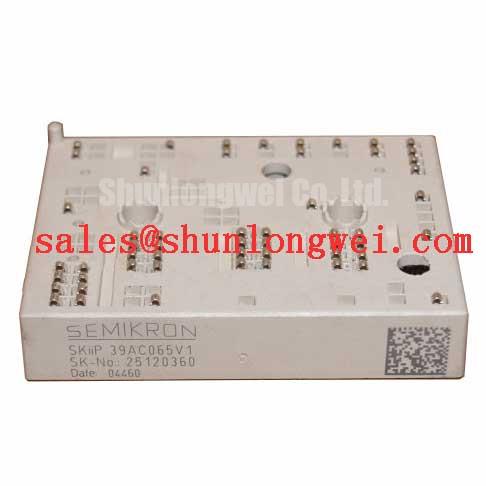
The Semikron SKIIP39AC065V1 is an IPM evaluated for industrial inverter service where electrical margin, switching behaviour, and heat removal must be assessed together. Its official ratings include 225 A continuous DC collector current at Tcase = 25°C, 720 W total power dissipation at Tcase = 25°C, and 0.04 K/W junction-to-sink thermal resistance per IGBT. At 150 A and 125°C junction temperature, the official typical collector-emitter saturation voltage is 2.2 V, with typical turn-on and turn-off energies of 5.7 mJ and 3.7 mJ.
| Official Datasheet Specification | Condition | Value |
|---|---|---|
| Collector-emitter blocking voltage, VCES | Tj = 25°C | 600 V |
| Continuous DC collector current, IC | Tcase = 25°C | 225 A |
| Total power dissipation, Ptot | Tcase = 25°C | 720 W |
| Collector-emitter saturation voltage, VCEsat | IC = 150 A, Tj = 125°C | 2.2 V typical |
| Turn-on energy, Eon | IC = 150 A, Tj = 125°C | 5.7 mJ typical |
| Turn-off energy, Eoff | IC = 150 A, Tj = 125°C | 3.7 mJ typical |
| Junction-to-sink thermal resistance, Rth(j-s) | Per IGBT | 0.04 K/W |
Long motor leads should be treated as transmission paths rather than as electrically invisible wiring. A PWM edge launched from an inverter can encounter an impedance discontinuity at the motor terminals and return as a reflected wave. Under certain cable, motor, and switching conditions, the terminal excursion can approach twice the DC-link voltage. This is a system phenomenon, not an additional voltage rating for the SKIIP39AC065V1; the official module boundary remains 600 V VCES.
Design Consideration: during repair or retrofit work, measure voltage at both the inverter output and the motor terminals with a measurement method appropriate for fast common-mode events. Compare the observed peak voltage, ringing frequency, and pulse repetition with a known-good axis where possible. A changing waveform can arise from cable length, motor winding condition, output filtering, grounding arrangement, probe connection, or gate-drive behaviour. It should not be assigned to a single cause without waveform evidence.
Where reflected-wave stress is significant, system engineers can assess an output dv/dt filter, sine-wave filter, or motor-output choke. Component selection must account for the motor cable, switching pattern, current spectrum, insulation system, and thermal duty. Physical spacing and routing also matter: keep motor phases together where practical, maintain orderly separation from sensitive feedback wiring, and avoid creating broad antenna loops between output conductors and the chassis.
The 2.2 V typical VCEsat at the stated official test point supports conduction-loss estimation, while the stated 5.7 mJ Eon and 3.7 mJ Eoff values help engineers understand switching-loss contribution at that same condition. Actual loss depends on the installed current waveform, junction temperature, gate-drive implementation, bus voltage, and switching frequency. For applications requiring a different voltage class, engineers may compare the electrical and mechanical requirements against the SKIIP37AC12T4V1 using the original equipment documentation rather than assuming interchangeability.
SKIIP39AC065V1 Circuit Protection & Reliability: Calibrating Differential Gate-Source Loop Routing
Gate-drive routing deserves inspection before a replacement module is energized. The power current path and the gate-source measurement path do not carry the same function. Shared inductance in a high-current emitter return can convert load-current transitions into unwanted gate-source voltage movement. This can alter the effective switching state, create ringing, or complicate interpretation of a desaturation protection event.
Design Consideration: route each gate command and its return as a compact differential loop, separated from the main high-current emitter path wherever the module interface and original circuit arrangement provide that option. The gate driver, its local decoupling, the control return, and any protection sensing should be reviewed as one switching loop. Keep high-current busbars short and geometrically balanced to reduce parasitic inductance that contributes to turn-off overshoot. The final layout must be verified by switching tests that compare peak device stress with the DC-link voltage and the official voltage boundary.
A desaturation-based short-circuit protection function, when included in the host drive, should be checked for correct blanking, sensing-path integrity, controlled gate turn-off behaviour, and fault-latch response. These settings are determined by the drive design and are not published operating prescriptions for this IPM. A controlled turn-off path can reduce abrupt current interruption, but its waveform must be validated against actual fault and load conditions.
When parallel power paths are under review, static sharing can benefit from the positive temperature coefficient of IGBT VCEsat in applicable operating regions, but that property alone does not ensure dynamic sharing. Symmetrical busbar geometry, matched gate paths, comparable thermal interfaces, and synchronized control remain necessary Design Considerations. For high-current driver boards, trace resistance and temperature rise should also be reviewed. Reference material on heavy copper PCB construction can assist with understanding conductor design choices, although the finished inverter board must be assessed as a complete system.
⚠️ Field Alert: Disconnect and verify the DC link is discharged before removing gate-drive or power connections, because stored energy can remain after the controller has been switched off.
SKIIP39AC065V1 Operational Boundaries: Evaluating Cres-Induced Gate Voltage Spike Limits
During a rapid collector-voltage transition, capacitively coupled current through the device capacitance network can raise the voltage of an off-state gate. If the gate loop has excessive impedance or shares a noisy return, the result can be unintended partial turn-on and shoot-through risk. This mechanism is particularly relevant when examining unexplained current spikes, irregular PWM waveforms, or asymmetric phase behaviour.
Engineering Recommendation: review the off-state gate path, local driver supply decoupling, control-ground return, and placement of an active Miller clamp if the host driver supports one. A negative off-state gate bias can improve immunity to induced gate voltage, but its magnitude, driver compatibility, insulation limits, and protection thresholds must be determined from the original drive documentation and confirmed during bench testing. It must not be selected from a generic module rule.
Use isolated differential measurement techniques where the test setup requires them, and keep probe ground connections from adding a large loop to the observed circuit. Inspect switching behaviour at realistic DC-link voltage and load conditions, while verifying the controller’s dead-time management and fault response. The official 600 V rating establishes a blocking-voltage limit, not a guarantee that every transient generated by a particular layout is acceptable.
For engineers comparing newer switching technologies while evaluating existing inverter constraints, the technical discussion in Wide Bandgap Revolution provides useful context on switching-speed trade-offs. Such comparison does not establish a direct replacement path for the SKIIP39AC065V1; package connections, protection architecture, thermal design, and control parameters require separate verification.
SKIIP39AC065V1 Thermal-Electrical Optimization: Thermal Cycling Margins of Internal Braking Practical Tuning
Motor deceleration returns mechanical energy toward the DC link. The drive-level braking arrangement must manage that energy without allowing the DC bus to rise beyond the limits of the assembled system. Whether braking is handled through an internal function, an external braking switch, a resistor assembly, or another energy-management method must be confirmed from the original drive schematic. The SKIIP39AC065V1 official data supplied here does not define a braking-resistor value, braking energy rating, or braking topology.
Design Consideration: evaluate the expected deceleration profile, reflected inertia, repeated-cycle duty, DC-link behaviour, and resistor thermal path as a combined energy-handling problem. Check resistor wiring for secure insulation clearance, inspect connectors for heat effects, and monitor bus-voltage behaviour during controlled deceleration tests. Repeated thermal cycling can expose weaknesses in heatsink contact, mounting flatness, thermal interface condition, or airflow long before a simple stationary resistance check identifies a concern.
The module’s official 720 W Ptot at Tcase = 25°C and 0.04 K/W Rth(j-s) per IGBT are essential inputs to a thermal assessment, but they do not replace calculation of actual conduction and switching losses for the installed operating cycle. Apply thermal interface material evenly according to the equipment manufacturer’s assembly instruction, use a clean flat heatsink surface, and validate temperatures under representative load transitions. Information on PTFE materials can be relevant when reviewing insulation and dielectric material choices around high-frequency assemblies, but it does not define this module’s internal construction or mounting requirements.
In a complete drive chain, upstream rectification and power-conditioning hardware can influence the DC-link response seen by the inverter. The SKM75GAL063D is a separate power-module option that may be reviewed as part of a broader rectifier-stage compatibility assessment. Its electrical ratings, topology, cooling arrangement, and control requirements must be evaluated independently.