

Content last revised on October 18, 2026
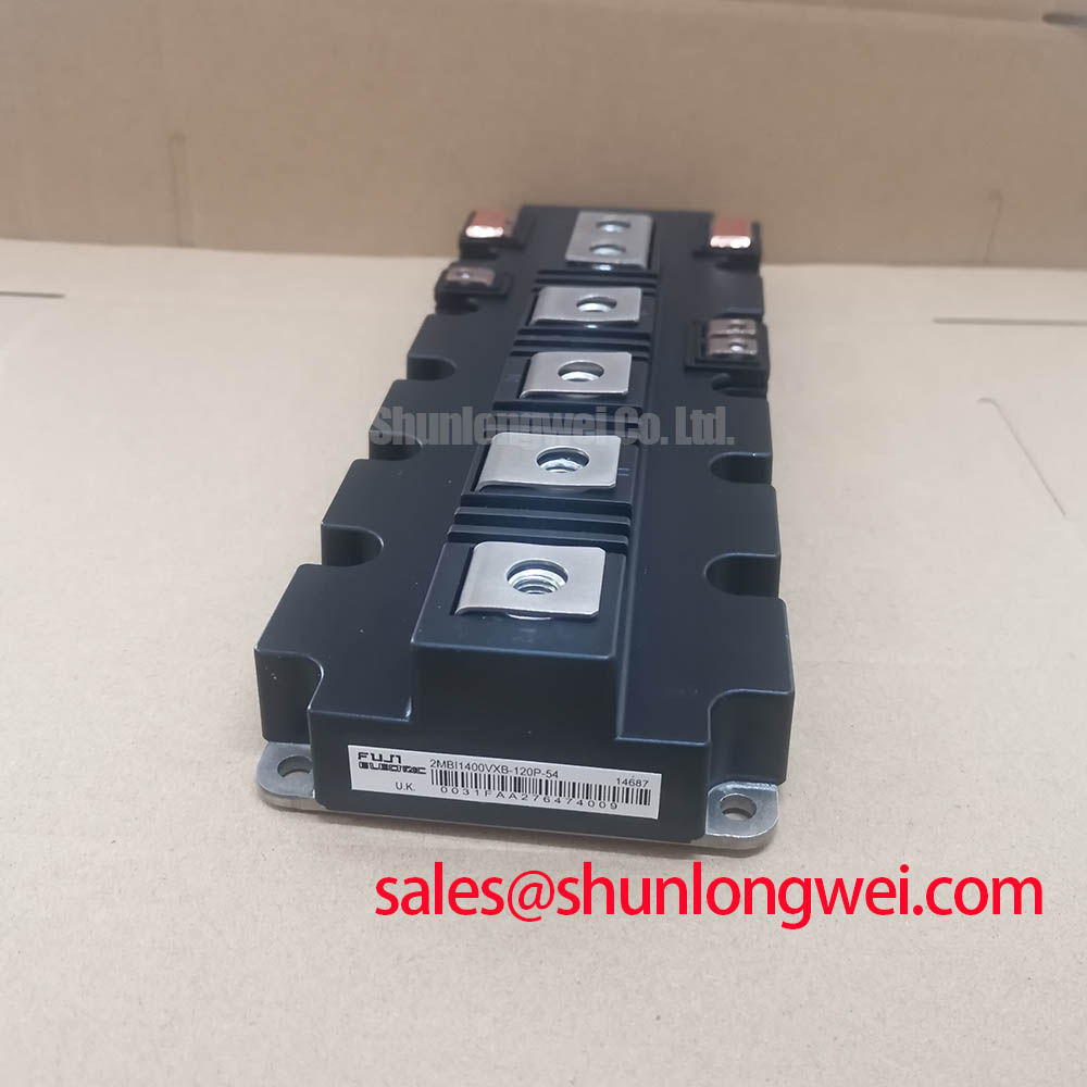
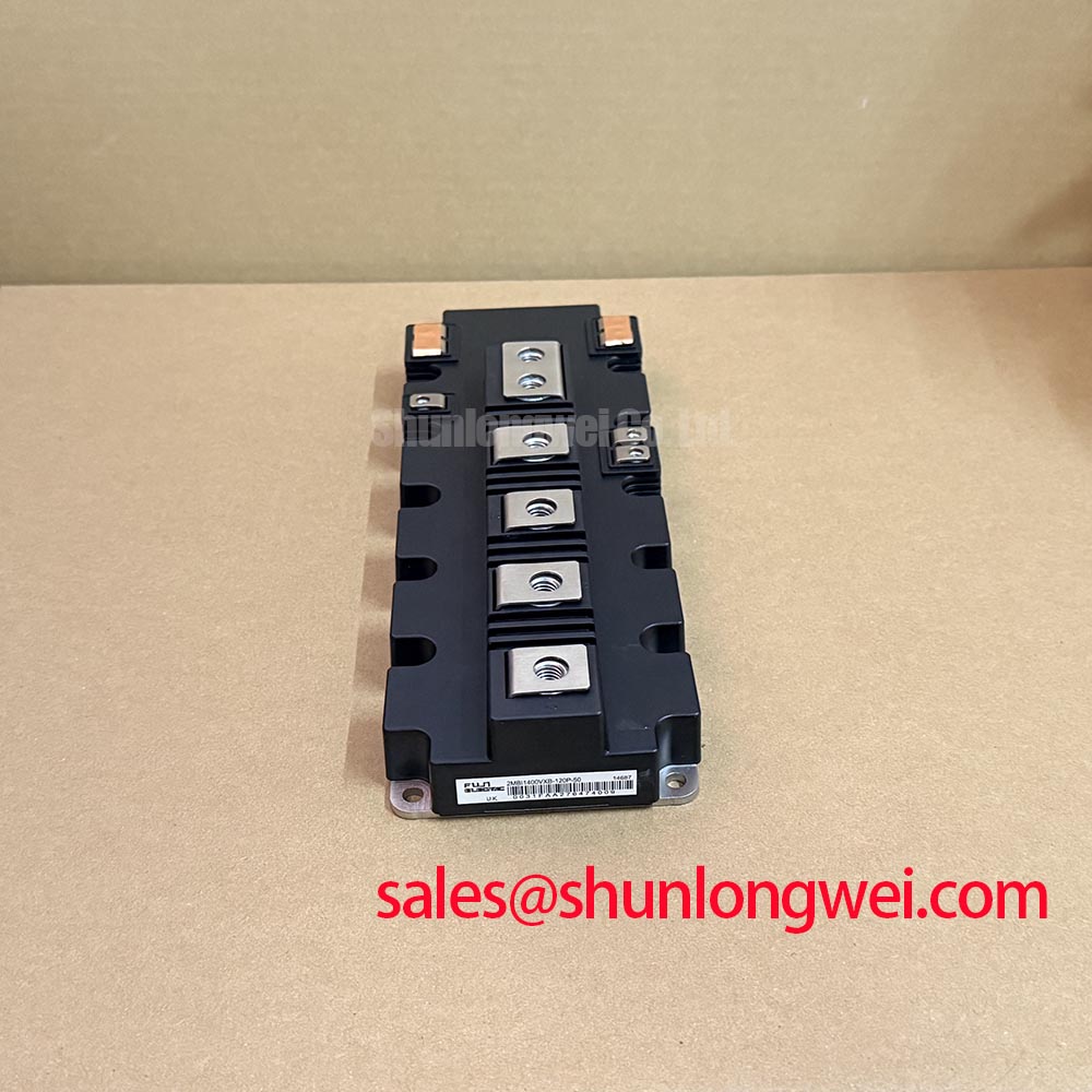
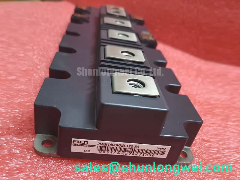
2MBI1400VXB-120-50 Circuit Protection and Reliability: Separating the Auxiliary Kelvin Emitter from the Main Power Emitter
With the DC link isolated, start a failed inverter investigation by checking the module’s main power terminals and gate return path for unintended continuity, then compare the wiring against the original driver layout. The Fuji Electric 2MBI1400VXB-120-50 is specified as a 1200.0 V, 1400.0 A IGBT module in a Fuji Power Module package. These are official product specifications; they are not a substitute for the switching, gate-drive, thermal, and transient limits required by the complete converter design.
The auxiliary Kelvin emitter connection must be treated as a driver reference, not as a convenient extension of the high-current emitter conductor. In a high-power PCS, the main emitter carries substantial commutation current while the auxiliary return is intended to give the gate driver a cleaner reference. If both returns share an uncontrolled copper path, the voltage developed by stray inductance can appear at the driver input as false gate movement. This can produce unexpected turn-on, excessive ringing, or an apparent mismatch between the commanded gate waveform and the voltage measured at the module terminals.
During field service, identify every gate, emitter, collector, and auxiliary return connection from the equipment drawing before removing wires. Do not infer a pin function from physical proximity alone. Trace the driver return to its actual termination, then inspect whether the high-current emitter cable, laminated busbar, shield, or measurement lead has been attached to that same point. The gate loop should be compact, with its outgoing and return conductors routed together to reduce loop area. Power commutation paths should remain physically separate from the sensitive gate-reference route while preserving the required creepage and clearance of the assembled system.
A practical commissioning check is to compare the gate-to-emitter waveform at the module interface with the signal at the driver output. A difference that appears only during high-current switching may indicate common-source inductance, probe-reference error, excessive loop area, or an incorrect auxiliary return connection. Use a suitable differential probe and a known-good phase leg for comparison. The final judgment should be based on measured gate overshoot, Miller plateau behavior, turn-off stability, and the system’s DC-link switching margin rather than on a resistance reading alone.
Gate-loop damping is a design consideration selected from the driver capability, gate charge, switching speed, parasitic inductance, and required loss balance. The correct value is system-determined. When the switching edge excites ringing, designers should evaluate gate resistance placement, driver sink capability, local decoupling, and the physical position of the return conductor before changing the protection threshold.
The module’s voltage and current ratings identify its product class, but they do not establish a universal operating point for every PCS topology. Designers should verify the actual bus voltage, modulation strategy, switching frequency, overload profile, cooling condition, and short-circuit protection response during controlled commissioning.
Assembly Integrity and Layout Architecture: Controlling Thermal Grease Pump-Out
Thermal interface preparation should begin with a clean inspection of the copper baseplate and heatsink contact surface. Look for high spots, embedded particles, burrs, old compound, and visible distortion along the mounting region. A baseplate that rocks on the heatsink can create local pressure concentration, while a heatsink with poor flatness can leave dry areas beneath the module. Both conditions increase thermal resistance and can encourage interface compound movement during repeated heating and cooling.
Use a suitable straightedge and a clean inspection method to assess the heatsink surface before applying thermal interface material. The compound should be spread as a thin, continuous film that fills surface irregularities without creating a thick insulating layer. The often-used 50 to 80 μm thermal interface target is a general industry design consideration, not an official 2MBI1400VXB-120-50 factory parameter. The material supplier’s application method and the module manufacturer’s mechanical guidance take priority.
Fasteners should be tightened progressively in a diagonal cross-pattern so that the module seats evenly instead of being pulled down from one corner. Use a calibrated tool and the fastening specification associated with the actual screw, washer, heatsink, and mounting arrangement. Do not transfer a torque value from another Fuji module or from a different bolt size. Excessive force can distort the baseplate or place mechanical stress into the module assembly, while insufficient force can leave an uneven thermal interface.
⚠️ Field Alert: Remove power and allow the DC link to discharge before touching the module or gate wiring, and never insert or remove a control connector while the converter is energized.
Switching frequency and ambient temperature should be considered together when assessing thermal headroom. A PCS operating at a lower switching frequency may still experience high semiconductor losses if current, modulation, overload duration, or cooling airflow is unfavorable. At higher switching frequencies, switching loss becomes a larger part of the heat balance. The suitable operating envelope must therefore be established from the complete loss model, heatsink performance, airflow condition, and measured case or heatsink temperatures.
| Engineering identification point | 2MBI1400VXB-120-50 | 2MBI50-120 |
|---|---|---|
| Manufacturer | Fuji Electric | Fuji Electric product family reference |
| Rated voltage | 1200.0 V | Confirm the part-specific rating before substitution |
| Rated current | 1400.0 A | Confirm the part-specific rating before substitution |
| Package description | Fuji Power Module | Confirm mechanical and terminal compatibility |
| Replacement decision | Match electrical, mechanical, thermal, and drive requirements | Do not treat the link as an automatic drop-in equivalent |
The linked 2MBI50-120 can be reviewed as a same-brand comparison point, but a replacement decision requires a complete check of voltage, current, terminal arrangement, gate characteristics, mounting dimensions, thermal interface, and protection coordination. Procurement teams should provide the equipment revision, nameplate information, and original connection drawing when requesting a compatibility review.
Field Diagnostics and Commissioning: Atmospheric Neutron Considerations for High-Altitude PCS Installations
For equipment installed above 2000 m, treat altitude as an application review item rather than applying an assumed neutron or voltage correction to the module. Atmospheric radiation exposure depends on altitude, location, shielding, operating time, and device technology. Single Event Burnout risk also depends on the applied electric-field conditions, switching state, transient behavior, and the device’s tested response. A numerical FIT or SEB prediction requires authoritative qualification data and a defined mission profile; it should not be generated from the 1200.0 V rating alone.
In a field investigation after an unexplained high-voltage failure, first separate an electrical overstress event from a possible environmental contribution. Inspect the DC-link record, precharge behavior, braking or clamp circuit, switching waveform, gate-drive supply, and protection reaction. Review whether the failure occurred during energization, regenerative operation, a load step, or a fault-clearing event. This timeline often provides more useful evidence than a post-failure resistance measurement, particularly when the semiconductor junction has already been damaged.
High-altitude installation also changes the surrounding system conditions. Reduced air density can affect cooling performance and external insulation coordination, while enclosure pressure, contamination, humidity, and cooling airflow influence the actual stress on the power stage. The system integrator should review the applicable equipment insulation and environmental requirements, then verify the DC-bus transient margin during representative switching tests.
For background on related Fuji Electric power-module architectures, engineers may consult the Fuji Electric Brake Chopper IGBT Modules reference and the Fuji Electric RC-IGBT Modules reference. Those product families should not be treated as evidence of identical construction, ratings, or environmental qualification for this model.
When the module is evaluated for a utility-scale centralized battery energy storage PCS, the service record should include DC-link voltage history, phase-current behavior, cooling conditions, gate-drive alarms, and the state of any clamp or snubber network. Designers should set protection and operating limits from the selected topology and verified test results, with special attention to transient voltage during turn-off and fault interruption.
Benchtop Waveform Tuning: Reducing Mechanical Stress Around Power Terminals
Before applying switching pulses on the bench, inspect the main terminal hardware for correct thread engagement, washer placement, conductor alignment, and signs of side loading. A stiff busbar that does not align naturally with the module terminal can act as a lever when tightened. That force may be transferred into internal joints or the base assembly, especially when the equipment later experiences vibration and thermal cycling.
Fit the busbar without forcing it into position, then confirm that the conductor remains flat against the terminal face throughout tightening. Washers should match the intended fastener system and should not bridge insulation barriers or interfere with adjacent terminals. The tightening sequence should maintain even contact pressure and avoid twisting the terminal block. If the terminal moves as the external conductor is secured, stop and correct the mechanical alignment rather than compensating with additional torque.
Waveform tuning should begin with a low-energy test condition that allows the engineer to observe gate voltage, collector-emitter voltage, current, and any clamp response. Gate-loop parasitic inductance can interact with the driver output resistance and gate charge, creating oscillation near the switching transition. The remedy may involve a shorter loop, improved driver return routing, carefully positioned damping, or a revised turn-on and turn-off strategy. The selected approach must preserve switching-loss limits and the driver’s protection timing.
Miller plateau charge and the effective reverse-transfer capacitance influence how readily a changing collector voltage couples into the gate circuit. Active gate clamping can be considered when the system requires additional control of unwanted gate rise during high dv/dt events, but the clamp threshold, response time, and layout must be validated against the actual driver and module behavior. Do not assume that a clamp arrangement tested on another IGBT module will provide the same result here.
For systems using negative off-bias, the driver supply, isolation barrier, gate resistor arrangement, and turn-off clamp must be assessed as one circuit. The technical discussion in Evolution of Negative Off-Bias Gate Drive Circuits provides a useful reference for evaluating that protection approach. The final gate voltage and timing remain system design choices and should be confirmed through controlled switching tests.
Finally, compare the measured transient behavior with the module’s documented surge, short-circuit, and thermal operating limits before increasing current or switching frequency. The 1400.0 A rated current is an official product parameter, not a blanket permission to use that current under every pulse width, junction temperature, cooling condition, or overload sequence.