





Content last revised on September 10, 2026
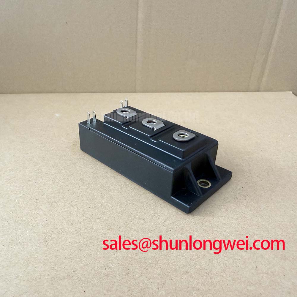
Before unboxing and mounting the 2MBI150PC-140-02 onto an inverter busbar assembly, field service technicians must perform an immediate static cold-state impedance screening across the power terminals. Measuring forward and reverse resistance between Collector and Emitter terminals using a calibrated digital multimeter in diode-test mode provides immediate confirmation of internal freewheeling diode health and gate oxide integrity. The dual-pack configuration of the Fuji Electric 2MBI150PC-140-02 requires verification that the high-side and low-side IGBT switches exhibit high input impedance across gate-to-emitter terminals without residual gate charge causing partial conduction during unpowered handling. Validating the baseline nameplate rating of V_CES = 1400V (Official Datasheet Specification) and continuous collector current capacity of I_C = 150A at T_c = 80°C (Official Datasheet Specification) ensures the replacement module satisfies the exact electrical voltage overhead demanded by high-bus power conversion stages.
| Parameter | Symbol | Official Specification | Unit |
|---|---|---|---|
| Collector-Emitter Voltage | V_CES | 1400 | V |
| Continuous Collector Current (T_c = 80°C) | I_C | 150 | A |
| Gate-Emitter Voltage | V_GES | ±20 | V |
| Maximum Power Dissipation | P_C | 1100 | W |
| Operating Junction Temperature | T_j | +150 | °C |
| Collector-Emitter Saturation Voltage (Typ / Max) | V_CE(sat) | 2.7 / 3.0 | V |
| Gate-Emitter Threshold Voltage (Min / Typ / Max) | V_GE(th) | 6.0 / 8.0 / 9.0 | V |
| Turn-on Time / Turn-off Time | t_on / t_off | 1.2 / 1.0 | µs |
| Thermal Resistance (Junction-to-Case, IGBT) | R_th(j-c) | 0.11 | °C/W |
| Thermal Resistance (Junction-to-Case, Diode) | R_th(j-c) | 0.24 | °C/W |
Benchtop Waveform Tuning: Mitigating Stress via Optocoupler vs Digital Coreless Transforme on 2MBI150PC-140-02
Isolating the low-voltage microprocessor control logic from the floating midpoint potential of a half-bridge module requires rigorous evaluation of common-mode transient immunity. When switching the 2MBI150PC-140-02 under high DC-link potentials, rapid voltage transitions generate substantial displacement currents through the parasitic coupling capacitance of the isolation barrier. High-speed optocouplers rely on internal Faraday shielding to achieve common-mode transient rejection, whereas digital coreless transformers employ differential capacitive or magnetic isolation structures to withstand high edge rates. In benchtop qualification, engineers must confirm that the galvanic isolation barrier maintains adequate voltage withstand ratings without permitting transient ground bounce to inject false turn-on pulses into the gate conditioning stage.
Signal propagation delays between top and bottom switches directly dictate the required hardware dead-time window. The 2MBI150PC-140-02 exhibits a factory turn-on time of t_on = 1.2 µs (Official Datasheet Specification) and a turn-off time of t_off = 1.0 µs (Official Datasheet Specification). To eliminate the risk of simultaneous bridge conduction, the gate driver circuit must incorporate deterministic dead-time generation alongside microsecond-level desaturation blanking filters. Comparing optoelectronic isolators against coreless transformer topologies reveals distinct propagation delay skews over operating temperatures; optocoupler LED degradation over service life can introduce timing drift, whereas digital isolation channels maintain tighter pulse-width distortion tolerances.
Mitigating Miller plateau induced cross-conduction is essential when switching inductive branch currents. As the complementary IGBT commutates, the high displacement current flowing through the reverse transfer capacitance can elevate the gate voltage above the minimum threshold voltage V_GE(th) = 6.0V (Official Datasheet Specification). Implementing an active Miller clamp circuit or maintaining a dedicated negative gate turn-off bias provides a low-impedance sink path, effectively shunting displacement currents away from the sensitive gate-emitter channel. When designing high-voltage solid-state conversion topologies, benchmark comparisons often reference wide-bandgap advancements detailed in The 1200 V CoolSiC™ MOSFET Advantage in Three for baseline switching performance under high dV/dt excitation.
Benchtop Waveform Tuning: Mitigating Stress via Evaluating Thermal Capacitance vs Heat Sin on 2MBI150PC-140-02
Dynamic thermal impedance determines the transient junction temperature rise under intermittent overload conditions. The 2MBI150PC-140-02 features a steady-state thermal resistance junction-to-case of R_th(j-c) = 0.11 °C/W (Official Datasheet Specification) for the IGBT section and R_th(j-c) = 0.24 °C/W (Official Datasheet Specification) for the integrated antiparallel diode. When subjected to transient short-circuit pulses or motor starting surges, the internal thermal capacitance of the silicon chip, direct bonded copper ceramic substrate, and copper baseplate absorbs the immediate energy burst before heat conducts into the external heatsink extrusion.
Modeling the transient thermal response requires representing the module as a multi-stage Foster or Cauer RC ladder network. In high-power conversion hardware, peak power dissipation can reach the maximum rated threshold of P_C = 1100W (Official Datasheet Specification), necessitating careful calculation of junction temperature margins relative to the upper operating limit of T_j = +150°C (Official Datasheet Specification). Desaturation detection circuits monitoring the on-state saturation voltage V_CE(sat) = 2.7V (Typ) / 3.0V (Max) (Official Datasheet Specification) must initiate a controlled two-stage soft turn-off sequence within microsecond-level fault windows to limit localized silicon overheating while simultaneously curtailing turn-off voltage spikes.
Active snubber networks paired with metal oxide varistors (MOV) across the primary DC bus terminals absorb stray inductive energy generated during high-speed current interruption. The relationship between DC-link busbar stray inductance and collector-emitter peak voltage dictates that minimizing busbar loop dimensions is necessary to maintain transient turn-off voltage peaks comfortably beneath the absolute maximum 1400V breakdown threshold. System integrators referencing complementary power conversion architectures and legacy retrofits frequently cross-evaluate modules such as the 2MBI150UC-120 to establish baseline thermal margins and package compatibility across distinct voltage classes.
2MBI150PC-140-02 Thermal-Electrical Optimization: Bi-Directional DC-DC Buck-Boost Conversion Practical Tuning
In bi-directional DC-DC converters operating between energy storage battery strings and centralized inverter buses, power flow transitions dynamically across all four operating quadrants. When functioning in boost mode during battery discharge, the low-side switch of the 2MBI150PC-140-02 handles active PWM switching while the high-side freewheeling diode provides continuous freewheeling conduction. Conversely, in buck mode during charging cycles, the high-side IGBT executes active switching while the low-side diode conducts the inductor current. This operational alternation distributes conduction and switching losses cyclically between the silicon dies, requiring balanced thermal distribution across the internal ceramic substrate.
Mitigating cyclic thermal swings during heavy charge-discharge cycling requires fine-tuning the gate drive resistor values and switching frequency. Increasing the turn-on series gate resistance dampens peak reverse recovery currents in the commutating diode, attenuating electromagnetic emission spikes at the expense of elevated turn-on switching energy. Parallel operation of multiple half-bridge modules for higher current throughput relies on the positive temperature coefficient of V_CE(sat) at elevated junction temperatures, which naturally promotes static current balance across paralleled channels by shifting current away from hotter dies.
Dynamic current sharing during sub-microsecond switching transitions depends heavily on symmetrical PCB trace layout and equalized gate driver loop lengths. Paralleled modules must experience identical parasitic inductances to prevent transient current crowding into a single device during high di/dt commutation. Advanced semiconductor packaging advancements and trench-gate characteristics are systematically documented across the Fuji Electric 7th-Gen X-Series IGBT Modules technical documentation, illustrating standard baseline architectures for high-reliability industrial power electronics.
Benchtop Waveform Tuning: Mitigating Stress via Thermal Interface Material Thickness Unif on 2MBI150PC-140-02
Achieving stable thermal transfer between the module baseplate and the system heatsink requires strict control over the thermal interface material application. Uneven grease thickness or dry spots introduce localized air pockets, significantly increasing contact thermal resistance and creating hot spots directly underneath the active IGBT dies. A uniform layer of high-conductivity thermal paste applied via screen printing or precision roller techniques ensures complete microscopic cavity filling without excessive hydrostatic pressure during mechanical assembly.
⚠️ Field Alert: Tighten baseplate mounting fasteners progressively in a cross-pattern sequence using an accurate torque wrench to achieve the standard industry mounting torque of 2.5 to 3.5 N·m, ensuring uniform paste spread without warping the copper baseplate.
Baseplate flatness and heatsink surface preparation directly impact thermal resistance contact values. Industrial heatsink mounting surfaces must meet stringent flatness specifications over the entire module contact area, preventing convex or concave air gaps from forming under the central ceramic direct bonded copper substrate. Verifying paste squeeze-out around the module perimeter after final fastener torque application confirms proper surface wetting and mechanical seating, securing long-term thermal conductance under continuous industrial power cycling.