Content last revised on October 3, 2026
2MBI200LB-060 Bench Verification & Product Identification
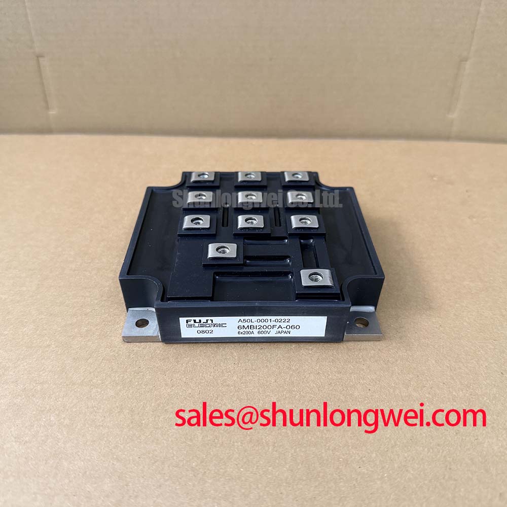
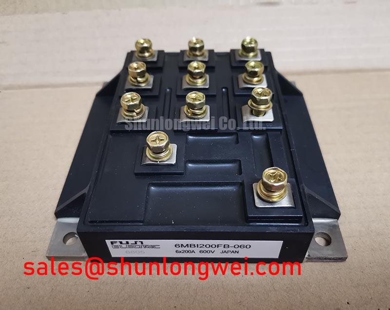
Begin bench verification with the drive isolated and discharged: inspect the Fuji Electric 2MBI200LB-060 module for cracked insulation, damaged terminals, loose hardware, and contamination before checking the power terminals with a meter. The official device data supplied for this product identifies a 600.0 V rated voltage, a 200.0 A rated current, and a module package. These ratings establish the component identity and electrical boundary, but they do not replace validation of the inverter’s DC link, switching conditions, cooling path, gate driver, and protection response.
| Parameter | Value | Engineering status |
|---|---|---|
| Manufacturer | Fuji Electric | Product identification |
| Part number | 2MBI200LB-060 | Product identification |
| Rated voltage | 600.0 V | Official specification |
| Rated current | 200.0 A | Official specification |
| Package | Module | Official specification |
For a heavy-duty variable frequency AC motor drive, replacement approval should begin with a comparison of the original electrical topology, terminal arrangement, gate-drive requirements, mounting pattern, thermal interface, and protection settings. The information above confirms the principal rating class only. The system integrator should verify every additional value from the original Fuji Electric documentation and the drive manufacturer’s service records before energizing the assembly.
2MBI200LB-060 Circuit Protection & Reliability: Calibrating Desaturation Detection
Desaturation protection is a system-level function, not an automatically guaranteed feature of the 2MBI200LB-060 module. During commissioning, confirm that the driver monitors the collector to emitter condition through a documented sensing path and that its response is coordinated with the gate command. The Fuji Electric V-Series IGBT Application Manual should be consulted for the applicable protection principles, switching limits, and gate-drive precautions. The final detection threshold, blanking interval, and shutdown response must be selected from the actual driver, DC-link, load, and fault-current behavior.
A short-circuit test should be treated as a controlled laboratory operation rather than a routine field check. Use the approved test fixture, current-limited energy source, isolated probes, and a documented stop procedure. The service engineer should observe gate voltage, collector-emitter voltage, phase current, and driver fault timing on the same event. A protection response intended for a fast fault must also avoid nuisance trips caused by switching transients, probe ground errors, or an unsuitable sensing layout. If the design target refers to a response below 10 microseconds or to a specific type-I or type-II short-circuit sequence, those requirements must be verified against the driver documentation and the relevant device application data rather than attributed to the module alone.
Two-stage soft turn-off can be considered where the gate driver supports it. The principle is to reduce the fault current in a managed way before completing the gate shutdown, limiting the interaction between stray inductance and the falling current. The correct timing remains system-determined. Engineers should capture the peak collector-emitter voltage during switching tests and compare it with the confirmed voltage rating and the drive’s transient limits. A soft turn-off sequence that is too slow may prolong fault stress, while an abrupt turn-off can increase inductive overshoot.
At the workbench, compare the suspect phase with a known-good phase under identical instrument settings. Check the gate command at the driver output and again at the module terminals, then inspect whether the fault signal is generated by the driver, the control board, or an external interlock. Unexpected protection activity may indicate wiring error, insufficient isolation, measurement interference, or a real power-stage fault. Do not declare the IGBT defective from a single oscilloscope trace; correlate the gate waveform with phase current and collector-emitter behavior.
Assembly Integrity & Layout Architecture: Implementing Symmetrical Busbar Geometry for High Current
The 200.0 A rating is an official product parameter, not a permission to operate at that current in every enclosure or duty cycle. Actual allowable current depends on switching frequency, case temperature, cooling arrangement, overload profile, busbar impedance, and the complete thermal design. When integrating this module into a variable frequency drive, keep the high-current path compact and physically balanced. Symmetrical busbar geometry helps reduce unequal stray inductance between parallel paths and can make current distribution more predictable during switching.
Static current sharing in parallel semiconductor paths can benefit from the positive temperature coefficient commonly associated with the on-state voltage of an IGBT at relevant operating conditions. This is a design consideration, not a substitute for measurement on the selected assembly. The engineer should compare current in each path at the intended operating temperature and load, while checking that gate wiring, emitter returns, busbar lengths, and thermal contact conditions are also matched. Dynamic imbalance can remain even when steady-state measurements appear acceptable.
Fuse coordination requires the same discipline. A high-speed semiconductor fuse should be evaluated against the module’s documented surge capability, the DC-link energy, the fault loop impedance, and the clearing behavior of the selected fuse. The fuse’s I²t value must not be treated as a standalone guarantee of module protection. Confirm the complete fault path with the fuse manufacturer’s data and a controlled fault study. Where the drive uses a braking chopper, regeneration path, or shared DC bus, include those energy sources in the assessment.
Mechanical assembly is part of the electrical result. The heat spreader should be clean and flat within the limits specified for the assembly, with an even thermal interface and no rocking of the module body. Use the fastening sequence and torque specified by the original mechanical design and fastener documentation. 🔧 Bench Diagnostic: Disconnect all power and verify the DC link is discharged before removing or inserting the module, gate cable, or phase connection.
For a related voltage-class comparison, engineers can review 2MBI200PB-140, but it should not be treated as a drop-in replacement without confirming voltage rating, terminal geometry, gate characteristics, thermal interface, and protection coordination. The comparison is a selection exercise, not a recommendation for substitution.
Assembly Integrity & Layout Architecture: Implementing Galvanic Gate Drive Isolation, Reinforced for 2MBI200LB-060
The gate driver must provide the isolation architecture required by the complete inverter. Reinforced isolation above 5 kV and common-mode transient immunity above 100 kV per microsecond are application requirements that must be confirmed from the selected driver and isolation components; they are not official specifications supplied here for the 2MBI200LB-060. The design team should verify creepage, clearance, insulation system, pollution environment, working voltage, and certification requirements as one coordinated barrier design.
Keep the isolated gate power loop and signal loop physically separated from the high di/dt collector and emitter paths. Minimize parasitic coupling while preserving the required safety spacing. The driver return should follow the documented module terminal arrangement, and any auxiliary emitter or sense connection must be used only when the relevant Fuji Electric terminal definition confirms its purpose. Do not infer a Kelvin emitter connection from the package appearance or from another IGBT family.
During fault investigation, monitor the isolated-side supply, gate command, gate-emitter voltage, and driver fault output with appropriately rated differential probes. A sporadic turn-on command may result from inadequate common-mode immunity, isolation capacitance, poor return routing, unstable isolated power, or control-board interference. Compare the timing of the command and the power-stage waveform before changing the gate resistance or protection threshold. The correct corrective action depends on the measured coupling path.
If the drive includes a rectifier or front-end power stage, the system topology may also be reviewed alongside 2MBI200UR-120-01. That reference does not establish compatibility with the 2MBI200LB-060; the engineer must verify the rectifier rating, DC-link behavior, precharge sequence, and protection coordination for the actual equipment.
Field Diagnostics & Commissioning: Differential Gate-Emitter Loop Routing to S in 2MBI200LB-060 Topologies
Commissioning should start with the gate loop, not with a higher control command. Use a differential probe across the gate and the correct emitter reference at the module terminals. A probe connected to an arbitrary chassis point can hide gate oscillation or create a misleading waveform. Record the command at the driver output and at the module so that cable inductance, connector contact resistance, isolation-stage delay, and reference movement can be separated during analysis.
Where the module documentation identifies a separate auxiliary emitter or low-inductance return, route that return independently from the main high-current emitter path. The purpose is to reduce mutual emitter coupling during rapid current transitions. If the exact terminal function is not confirmed, the system integrator should consult the original Fuji Electric documentation rather than assuming a pin assignment. Keep gate and emitter conductors closely coupled over their intended route, while maintaining the required insulation spacing from the collector and DC-link conductors.
Oscillation, uneven switching, or repeated driver faults should be investigated through waveform comparison. Check the gate amplitude, turn-on and turn-off transitions, the emitter reference movement, and the collector-emitter overshoot under the same load condition. Potential contributors include excessive loop inductance, an unsuitable gate resistor, driver supply instability, connector movement, contamination, or an incorrect terminal reference. Any change to damping or gate resistance should be treated as a typical starting point for bench tuning and validated against switching loss, fault response, and peak voltage.
For higher stress evaluation, engineers may use the Power Electronics Masterclass as a supplementary reference for measurement planning and system reliability review. The final acceptance decision should come from recorded tests on the intended drive assembly, including cold start, thermal stabilization, load transients, fault shutdown, and repeated start and stop operation.