Content last revised on October 31, 2026
MG200Q1US51 Specifications and Replacement Checks
- Isolate the equipment, verify that the DC link is discharged, and compare cold collector-to-emitter and gate-to-emitter measurements with the circuit diagram and a known-good assembly.
- Inspect the module mounting surface, terminal hardware, and heatsink contact area for contamination, distortion, or evidence of uneven seating.
- Check gate-drive connections and isolation barriers before reconnecting the power stage; distinguish module measurements from parallel paths through the surrounding circuit.
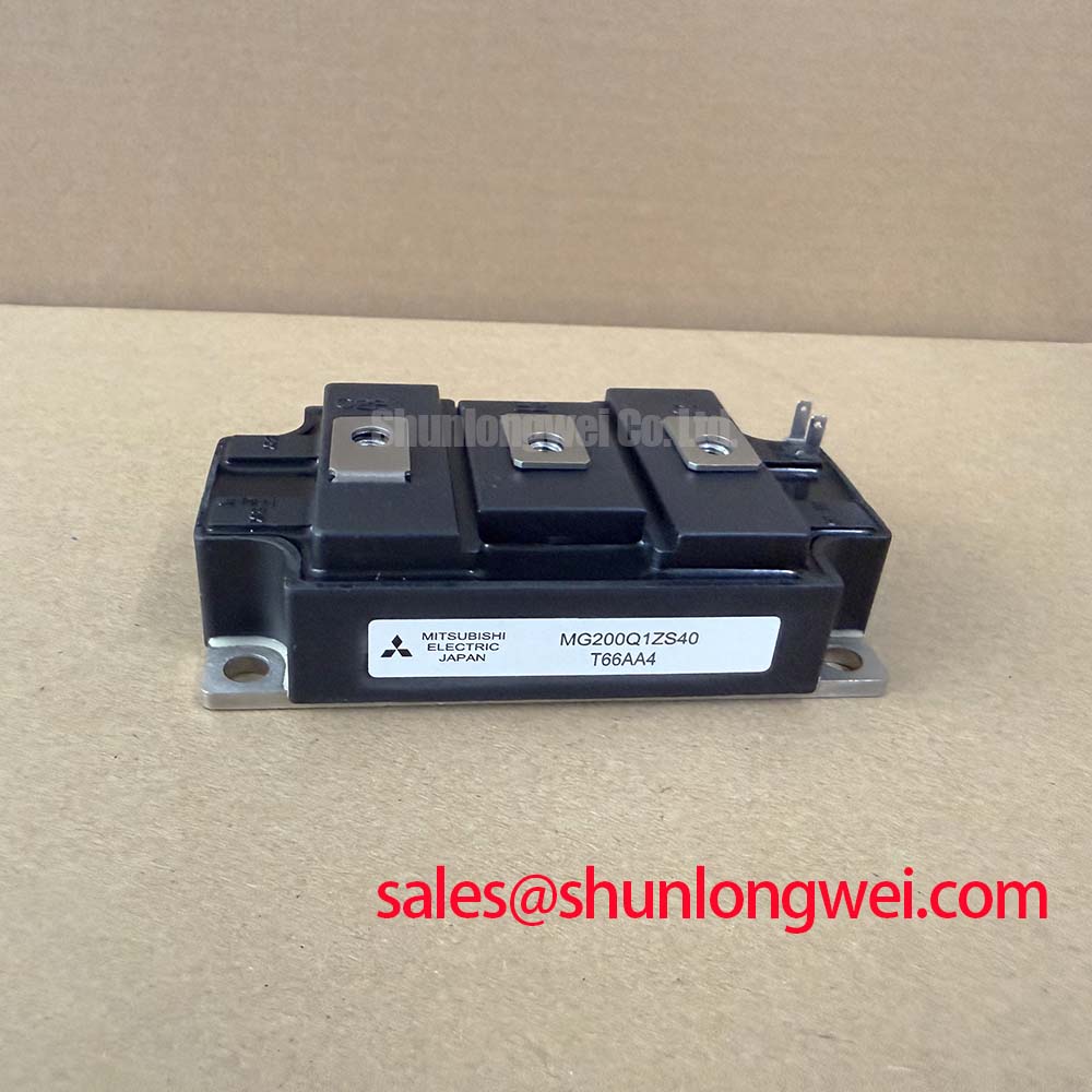
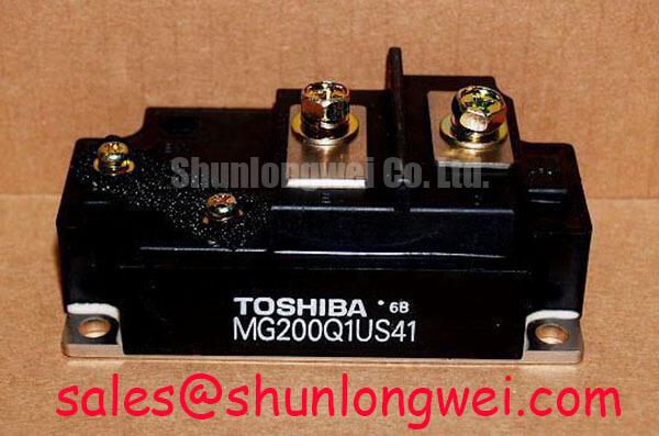
- Match the full MG200Q1US51 designation, circuit arrangement, and mechanical interfaces before authorizing replacement.
The Toshiba MG200Q1US51 is a 1200 V, 200 A IGBT module with a single-switch configuration. The specification card below separates its electrical and thermal ratings from the system-dependent installation decisions discussed afterward. Switching conditions, terminal assignments, mounting dimensions, and rating test conditions belong in the replacement approval checklist.
| Parameter | Official Specification | Engineering significance |
|---|---|---|
| Collector-emitter voltage, VCES | 1200 V | Blocking-voltage boundary for assessing measured switching stress. |
| Continuous collector current, IC | 200 A | Current rating subject to its specified thermal and operating conditions. |
| Typical collector-emitter saturation voltage | 3.0 V | Conduction-loss reference; not a guaranteed value at every operating point. |
| Maximum junction temperature | 150°C | Junction-temperature limit, not a recommended continuous operating target. |
| Junction-to-case thermal resistance | 0.12°C/W | Thermal-path parameter that excludes the external mounting interface and heatsink. |
| Circuit configuration | Single-switch, one-pack | Configuration to match against the equipment schematic. |
Assembly Integrity & Layout Architecture: Implementing Output Sinusoidal Filter vs dv/dt Reactor for MG200Q1US51
Compare switching-edge waveforms at the inverter output and load terminals before attributing a long-cable overvoltage to the module. Design Consideration: cable propagation and impedance discontinuities can produce reflected voltage waves, so load-terminal stress and collector-emitter stress require separate measurements. Use suitably rated differential probes and control probe-loop pickup; an unsuitable measurement arrangement can obscure the distinction between actual overshoot and measurement artefacts.
A dv/dt reactor or filter primarily addresses edge-related stress, while a sinusoidal output filter attenuates switching-frequency content more extensively. Selection should account for cable length, load characteristics, switching frequency, fundamental frequency, filter losses, and control-loop interaction. The MG200Q1US51 current rating alone does not establish the required inductance or capacitance. Filter acceptance should follow loaded measurements and the equipment manufacturer's permitted output-network arrangements.
During reassembly, preserve separation between power conductors and gate-drive wiring. Route outgoing and returning power paths to limit unnecessary loop area, while retaining the equipment's required electrical clearances. Inspect added reactors for overheating, loose connections, and installation changes that could alter their behaviour. A filter should not conceal unstable gate drive or excessive commutation-loop inductance.
For replacement comparisons, treat the MG50H1BS1 as a separate component requiring an independent voltage, current, topology, drive, and mechanical review—not as a drop-in substitute. Potential evaluation contexts for the MG200Q1US51 include industrial inverter welders and medium-frequency induction-heating supplies, subject to their actual switching and cooling requirements; motor-cable filtering applies only where the equipment topology calls for it.
Transient Dynamics & Electrical Design: Type-2 Coordination and Protection of the MG200Q1US51 IGBT Module
Separate semiconductor protection from upstream fault interruption when reviewing a failed power stage. Design Consideration: a high-speed fuse can limit fault energy, but its total clearing I²t cannot establish IGBT survival without compatible semiconductor withstand information and circuit-specific fault analysis. DC-link capacitor discharge, available fault current, circuit inductance, and fuse DC interruption capability all influence the event.
Type-2 coordination terminology should not be treated as an intrinsic certification of this module. Establish the equipment's applicable coordination requirements and assess the complete protective combination. Neither a current-rating match nor a fuse catalogue comparison guarantees prevention of enclosure damage. Check the capacitor bank, bus connections, gate-driver fault response, and upstream protective devices as an interacting assembly.
Gate-driver desaturation detection and controlled shutdown address a different timescale from fuse operation. Review fault blanking, driver supply behaviour, and shutdown waveforms against the actual switching conditions. Common-mode transients across an optocoupler or digital isolator can disturb control signals, so compare the isolator's specified immunity with measured switching-node behaviour and the surrounding layout.
Where equipment uses parallel modules, symmetrical power paths and comparable thermal interfaces support current sharing. Do not assume that a positive temperature coefficient applies throughout the operating range merely because the device is an IGBT. Assess the relevant output characteristics and compare branch currents during both conduction and switching. The 3.0 V typical saturation voltage is not a current-sharing tolerance or a device-matching specification.
For broader switching-loss context, Unlocking Efficiency in Industrial Drives discusses another IGBT technology generation; its device-specific characteristics must not be transferred to the Toshiba module or used as its protection acceptance criteria.
Transient Dynamics & Electrical Design: Turn-Off di/dt-Induced Peak Voltage and Clamping for MG200Q1US51
Capture collector-emitter voltage during turn-off at representative current, DC-link voltage, and temperature before changing a snubber. Engineering Calculation: the first-order relationship Vpeak ≈ VDC + Lσ × |di/dt| explains how commutation-loop inductance adds voltage stress as current falls. It is a screening model rather than a complete prediction of ringing, diode recovery, or clamp behaviour.
Reduce unnecessary commutation-loop area through closely coupled outgoing and return conductors, short capacitor connections, and consistent terminal geometry. Busbar changes must preserve clearance and insulation requirements. The acceptable inductance follows from the measured switching behaviour and voltage budget; imposing an arbitrary universal inductance target can overlook terminal geometry or create mechanical compromises.
Snubber selection requires attention to pulse current, repetitive dissipation, connection inductance, and the energy transferred during commutation. Positioning matters because a remote capacitor may provide little control over a local high-frequency loop. Evaluate damping and temperature together: suppressing a visible oscillation does not establish that the snubber remains within its electrical and thermal ratings.
Inspect the gate waveform alongside collector-emitter voltage. Miller coupling can disturb the off-state gate, while driver impedance and return-path inductance influence the response. Active clamping and gate-resistor changes should be evaluated as coordinated protection measures, with switching loss and unintended turn-on checked during testing. Reverse-recovery behaviour also affects commutation stress; do not assign a diode softness factor or surge-current capability without the relevant device data.
Where regenerative operation is present, assess DC-link energy management separately from turn-off overshoot. A braking resistor or chopper addresses a different energy path from a local snubber. Measure both the slower bus-voltage rise and the fast switching excursion rather than expecting either protection mechanism to resolve both.
Benchtop Waveform Tuning: Heatsink Contact Pressure and Thermal Checks for MG200Q1US51
Inspect the heatsink contact surface and module base before tightening the mounting hardware. Design Consideration: contamination, uneven seating, and an unsuitable thermal-interface application can increase case-to-heatsink thermal resistance even when the module's internal thermal path remains unchanged. The specified 0.12°C/W junction-to-case resistance does not include those external contributions.
Apply the thermal-interface material using its qualified process and the module's mounting instructions. Seek continuous contact without unnecessary excess material, and inspect the contact pattern where the service procedure permits. Interface thickness depends on surface condition, material behaviour, and assembly tolerances; it should not be assigned a universal value for this module. Do not force a visibly distorted assembly flat through additional screw loading.
Field Alert: Tighten mounting hardware in the prescribed sequence and to the applicable mounting specification, rather than using extra torque to compensate for poor heatsink contact.
Packaging-material properties are not evidence of this module's internal construction. References on eutectic systems explain alloy phase behaviour, while polyphenylene sulfide describes an engineering polymer. Neither establishes the MG200Q1US51 die-attach alloy, housing material, or permissible mounting process.
During controlled loading, correlate case-temperature measurements with cooling conditions and estimated losses. The 150°C maximum junction temperature is not a case-temperature acceptance limit. Repeat waveform observations after thermal stabilisation, checking whether gate behaviour, overshoot, or current distribution changes as the assembly warms. Record load, coolant or airflow condition, measurement locations, and shutdown response so the repaired assembly can be assessed against the equipment's own acceptance procedure.