Content last revised on September 10, 2026
2MBI200S-120-02 Specifications and Inspection
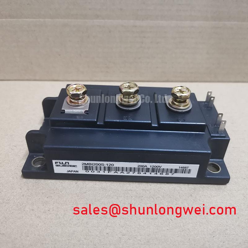
With the converter de-energized and the DC link confirmed discharged, begin incoming inspection by checking the terminal layout against the equipment schematic, then compare collector-emitter and gate-emitter readings across the installed positions under the same meter conditions. The 2MBI200S-120-02 is a Fuji Electric IGBT module rated at VCES 1200 V and IC 200 A at TC 80°C, according to the official specification. Its stated gate-emitter limit is ±20 V, maximum specified junction temperature is 150°C, and total power dissipation is 1040 W per device at TC 25°C.
| Official Specification | Condition | Value |
|---|---|---|
| Collector-emitter voltage, VCES | Tj = 25°C | 1200 V |
| Continuous collector current, IC | TC = 80°C | 200 A |
| Collector-emitter saturation voltage, VCE(sat) | IC = 200 A, VGE = 15 V, Tj = 25°C | 2.2 V typical, 2.7 V maximum |
| Gate-emitter voltage, VGES | Absolute maximum rating | ±20 V |
| Power dissipation, PC | TC = 25°C, one device | 1040 W |
| Junction-to-case thermal resistance, Rth(j-c) | IGBT, maximum | 0.12°C/W |
| Short-circuit withstand time, tsc | VCC = 600 V, VGE ≤ 15 V, Tj = 125°C | ≥10 µs |
| Junction temperature, Tj | Maximum specified value | 150°C |
💡 Bench Tip: Keep the module and test lead assembly protected from ESD and record cold-state readings before applying any gate-drive or high-voltage test stimulus.
Benchtop Waveform Tuning: Mitigating Stress by Suppressing 2× VDC Voltage Doubling in 2MBI200S-120-02
At commissioning, a voltage probe should be placed at the module-side DC terminals and the motor-side waveform should be observed separately when lead length is substantial. A long motor cable can behave as a transmission path rather than a simple conductor. If its characteristic impedance and the motor input impedance are mismatched, reflected wavefronts can add to the original switching step. Under particular cable, load, and edge-rate conditions, this reflection mechanism can approach twice the DC-link voltage at a remote terminal. This is a system behavior, not an additional voltage rating of the 2MBI200S-120-02.
The official 1200 V VCES rating is the electrical boundary that must be respected at the IGBT. Engineers should capture peak collector-emitter voltage with probe placement and bandwidth appropriate to the switching event, then compare the result with the measured DC-link condition. Waveform ringing, a remote motor-terminal overshoot, and a collector-emitter peak are related but are not interchangeable measurements. Checking all three prevents a cable-related event from being misread as an inherent module defect.
A Design Consideration is to minimize the distance between the switching module and its DC-link decoupling path, while treating output cable routing, filter placement, and motor cable shielding as a coordinated system. Output reactors and dv/dt filter networks can reduce the rate and amplitude of wavefronts delivered to long leads, but their selection depends on motor insulation, cable construction, PWM strategy, load current, and measured waveform behavior. The system engineer should validate the resulting voltage peaks under the highest relevant DC-link and operating conditions.
For industrial inverter welders or medium-frequency induction-heating power supplies, do not assume that a stable no-load waveform proves a satisfactory switching environment. Recheck the trace while the intended process load is active. A change in ringing frequency, peak voltage, or gate waveform may indicate an altered current loop, probe grounding artifact, cable effect, or load-dependent commutation condition. Where an equipment repair requires a parameter comparison rather than an automatic replacement decision, the 2MBI200PB-140 can be reviewed against its own published electrical ratings, package arrangement, gate-drive requirements, and mechanical drawing.
Preventing Spurious Faults: Turn-Off di/dt-Induced Vpeak Clamping and Guidelines for 2MBI200S-120-02
During turn-off, the collector-emitter peak arises from the DC-link voltage plus the voltage developed across stray inductance by changing current. In engineering terms, the added portion follows the relationship of loop inductance multiplied by current slew rate. This explains why a circuit can produce a high peak even when its steady DC-link reading appears well controlled. The relevant loop includes the module terminals, bus structure, capacitor connection, and current return geometry.
Design Consideration: Keep the commutation path compact and geometrically paired so outgoing and return currents remain close together. A symmetrical laminated or planar busbar approach is commonly evaluated to reduce loop inductance, while unequal paths can cause different switching stress between positions. Snubber capacitors can be part of the solution when selected from measured energy, voltage, ripple-current capability, and layout effectiveness. Their physical location and connection inductance matter as much as nominal capacitance.
The 2.2 V typical and 2.7 V maximum VCE(sat) values apply only at the official condition of 200 A, 15 V VGE, and 25°C Tj. They are useful for static comparison, but they do not quantify switching loss at a specific PWM frequency. At higher switching frequency, switching energy, current waveform, gate drive, cooling performance, and load duty determine the thermal result. The official 0.12°C/W maximum junction-to-case thermal resistance for the IGBT provides one part of the thermal path; interface material, heatsink flatness, clamp force, airflow, and ambient conditions remain system-determined.
When an inverter trips only after a loaded interval, capture collector-emitter voltage, current, gate-emitter voltage, and heatsink temperature during the same operating sequence. A protection event can result from legitimate overcurrent detection, a false gate-drive disturbance, insufficient cooling, measurement pickup, or transient voltage stress. Avoid interpreting one waveform in isolation. The stated tsc ≥10 µs rating applies specifically at VCC 600 V, VGE ≤15 V, and Tj 125°C; it should not be treated as a permitted fault duration for a different bus voltage, junction temperature, or protection circuit.
2MBI200S-120-02 Circuit Protection & Reliability: Calibrating Optocoupler vs Digital Coreless Transformer
Before connecting a replacement module to a driver board, verify the original gate and emitter terminal assignment from the equipment documentation and inspect the driver output with the power stage isolated where the service procedure permits. A diode-mode check can reveal an unexpected conductive path or inconsistent reading between comparable inverter positions, but it cannot certify switching performance. Gate-emitter readings must also be interpreted in relation to the installed driver, parallel components, and any protection network still connected to the circuit.
Galvanic isolation is a driver-system requirement rather than an official specification stated for this module. Engineering Recommendation: assess the required isolation barrier and common-mode transient immunity from the equipment’s DC-link voltage, expected switching edges, control architecture, and applicable safety requirements. Optocouplers and digital coreless-transformer isolators have different propagation, noise-immunity, bias-supply, and fault-state behaviors. Neither device category is automatically suitable solely because it appears in another inverter design.
Spurious turn-on symptoms should be investigated by viewing the gate-emitter waveform at the relevant module reference, not solely from a controller-side ground. Check whether the gate signal changes during the opposite device’s switching transition, whether the driver supply remains stable, and whether the return path shares high-current switching current. Separation of sensitive gate-drive routing from power commutation loops is a practical Design Consideration for reducing coupled noise. The final arrangement should be verified on the assembled equipment under representative load conditions.
For product-family context and current Fuji Electric power-semiconductor information, consult Fuji Electric 7th-Gen X-Series IGBT Modules and Fuji Electric RC-IGBT Modules. These references should not be used to transfer unlisted ratings, pin assignments, isolation claims, or switching characteristics to the 2MBI200S-120-02.
Field Diagnostics & Commissioning: Sizing Braking Resistors and Chopper Trans in 2MBI200S-120-02 Topologies
When a motor decelerates, its kinetic energy can return to the DC link. In a topology using a braking chopper, the chopper switch and braking resistor must absorb or redirect that energy according to the equipment design. The 2MBI200S-120-02 should be evaluated only in the topology documented for the original converter; the official parameters provided here do not establish that it is the braking device, nor do they specify a resistor value, pulse-energy rating, or chopper current limit.
For commissioning, observe the DC-link response during controlled deceleration and correlate it with the braking command, resistor temperature behavior, and protective-fault record. If the DC link rises unexpectedly, inspect the chopper command path, resistor continuity, wiring terminations, and current sensing before assigning the event to the IGBT module. If a chopper conducts continuously, examine the driver command state, feedback circuitry, and controller logic as well as the power stage. These checks preserve the distinction between a power-device symptom and a control-system cause.
In related converter architectures, the 2MBI200UR-120-01 may be considered as a separate device reference for front-end or auxiliary-stage documentation review. Its presence in a system does not establish electrical interchangeability with the 2MBI200S-120-02. Verify circuit role, voltage rating, current rating, terminal arrangement, gate-drive interface, thermal path, and original equipment requirements before making a service decision.
After installation, repeat the cold-state terminal checks, confirm that mounting surfaces are clean and planar, and monitor the first energized run with the intended protection functions active. Record DC-link voltage, load current, collector-emitter waveform, gate waveform, and cooling response as a commissioning baseline. For broader practical context on checking power-semiconductor use in industrial equipment, see Industrial Applications.