Content last revised on September 23, 2026
2MBI200S-120-52 Operational Boundaries: Evaluating SCSOA Overcurrent Protection
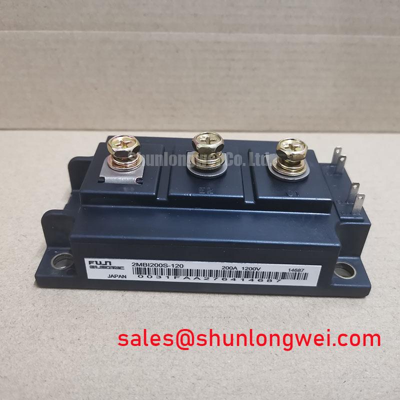
Start the bench check with the equipment isolated, then inspect the 2MBI200S-120-52 case, terminals, baseplate, and mounting area for cracks, contamination, loose hardware, or signs of thermal stress before applying any test voltage. Confirm the replacement marking against the failed unit and verify the inverter or energy storage converter’s electrical limits against the manufacturer’s documented ratings.
| Characteristic | Symbol | Rated Value | Classification |
|---|---|---|---|
| Collector emitter voltage | VCES | 1200 V | Official specification |
| Continuous collector current | IC | 200 A | Official specification |
| Pulsed collector current | ICP | 400 A | Official specification |
| Specified collector power dissipation | PC | 1500 W under datasheet conditions | Official specification |
| Maximum junction temperature | Tj | 150 °C | Official specification |
| Isolation voltage, AC for 1 minute | VISO | 2500 V | Official specification |
The 1200 V collector emitter rating and 200 A continuous collector current rating define important device boundaries, but they do not by themselves establish a safe short circuit operating area for every converter topology. In a commercial string inverter or micro grid energy storage system, the protection circuit, gate driver, DC link, busbar arrangement, and current sensor response must be assessed together.
For a field replacement, begin with a cold resistance and diode path comparison against a known good assembly when the circuit allows safe isolation. A shorted collector emitter path, an abnormal gate terminal reading, or a damaged auxiliary connection can justify removing the module for controlled bench testing, but none of these observations should be treated as a complete failure diagnosis without checking the surrounding gate driver and commutation network.
Short circuit protection should detect abnormal current promptly and coordinate with the driver’s turn off behavior. A two stage soft turn off approach is a Design Consideration rather than a documented specification of this module. The first action limits uncontrolled current, while the second reduces gate drive energy in a controlled way to reduce the risk of inductive overvoltage. The actual detection delay, blanking interval, desaturation threshold, and soft turn off profile must be selected and validated by the system designer.
During commissioning, use a current probe and a properly rated differential voltage probe to observe the collector emitter waveform during startup, controlled load steps, and fault simulations. Check the peak voltage against the system DC link and the 1200 V device rating. If the waveform approaches the device boundary, investigate loop inductance, gate resistance, clamp behavior, and sensor timing instead of assigning the stress to the IGBT module alone.
Clearance and creepage around the high voltage switching path should follow the applicable system insulation standard and enclosure pollution environment. The module’s 2500 V AC for 1 minute isolation rating is an official module specification; it is not an automatic certification of the complete inverter, battery converter, or cabinet. The system integrator should validate reinforced insulation, protective barriers, and dielectric test procedures at assembly level.
For maintenance teams comparing compatible inventory, the 2MBI200PB-140 may be evaluated as a separate Fuji Electric device, subject to confirmation of electrical ratings, terminal arrangement, mechanical fit, gate drive requirements, and the original equipment documentation. It should not be treated as an automatic substitute solely because the current rating appears similar.
Benchtop Waveform Tuning: Isolated Gate Power and Interlock Checks
Before connecting a replacement module to a live power stage, test the isolated gate driver independently. Confirm that the isolated DC to DC supply has the required galvanic isolation for the complete control assembly and that its transient immunity is appropriate for the switching environment. Values such as reinforced isolation voltage and common mode transient immunity belong to the selected gate driver and power supply design; they are not published ratings of the 2MBI200S-120-52.
Observe the gate supply during repetitive switching rather than checking only its no load value. The bootstrap or isolated gate supply capacitor must retain adequate charge during the intended pulse pattern, while the charging diode must recover cleanly at the operating frequency and voltage. A falling gate supply, ringing supply rail, or delayed recharge can create incomplete turn off and unwanted overlap between complementary switches.
Use a complementary gate interlock in the driver logic and verify the actual gate emitter waveforms at the module terminals. Dead time is system determined. It must account for driver propagation mismatch, turn off delay, module switching behavior, temperature, and the measured response of the complete power stage. Adding dead time without checking current commutation can increase diode conduction and switching loss, so the final value should be confirmed with waveform measurements.
Keep the gate return path separate from high current power conductors. If the selected module provides an auxiliary emitter or sensing connection, the system integrator should verify its exact terminal function from the original Fuji Electric documentation before routing the PCB or busbar. A Kelvin style return can reduce the influence of common emitter impedance, but the terminal assignment and permitted connection method must be confirmed for the actual module drawing.
The same practical method applies when a gate fault appears after replacement. First isolate the driver output, then inspect the gate resistor, clamp network, isolated supply, interlock signal, and cable routing. An oscilloscope comparison with the known good channel can reveal impedance mismatch or common mode coupling more reliably than a resistance test alone. The external RS 485 differential bus used elsewhere in an industrial controller should also be kept away from high dv/dt gate and power switching routes.
Field Alert: Disconnect the DC link and verify the discharge state before removing gate or power connections, because control wiring can remain exposed to hazardous potential after the main switch is opened.
Assembly Integrity and High Frequency Commutation Loop Architecture
After electrical screening, inspect the baseplate contact area and the heatsink surface for burrs, foreign particles, unevenness, or old thermal interface material. The objective is uniform thermal contact across the baseplate, not a thick layer of compound. A thin, even application selected for the heatsink finish and pressure distribution is a Design Consideration; the exact interface material and application thickness should follow the equipment service documentation.
Mounting pressure must be applied progressively and evenly according to the fastener specification and the equipment manufacturer’s assembly procedure. Excessive pressure can distort the mounting interface, while insufficient pressure can increase thermal resistance and allow mechanical movement during thermal cycling. The 1500 W maximum collector power dissipation rating does not remove the need to verify heatsink performance, airflow, coolant conditions, and the actual power loss of the switching pattern.
Keep the high frequency commutation loop compact. The path from the DC link capacitor through the module and back to the capacitor should use a symmetrical laminated or planar arrangement where practical. The turn off overshoot is influenced by stray inductance and current slew rate; in engineering terms, the peak voltage rises with the product of loop inductance and di/dt. The system designer must measure the resulting peak at the module terminals and compare it with the DC link operating condition and the 1200 V rating.
Snubber capacitors, clamp networks, and MOV protection should be coordinated rather than selected as isolated parts. An MOV can absorb surge energy outside the normal switching event, while a local snubber can control a faster commutation transient. The voltage class, pulse energy, repetitive duty, placement, and thermal environment must be calculated from the actual converter waveform. No MOV or snubber value can be assigned to this module from the six published ratings alone.
Check the physical distance between the power terminals, gate wiring, auxiliary connections, and nearby control traces. Avoid routing a sensitive gate return alongside the collector or emitter bus for long parallel distances. When an industrial inverter uses a battery bidirectional DC to DC stage, repeated charge and discharge operation can increase thermal cycling in the module, busbar, interface material, and soldered connections. Designers should evaluate the complete thermal cycle profile rather than infer service life from the module’s current rating.
For system level architecture references, the article Unlocking Efficiency in Industrial Drives provides additional context on switching efficiency and power semiconductor design. It should be used as engineering background, while the Fuji Electric documentation remains the authority for this exact part’s terminal definition and ratings.
Field Diagnostics and Commissioning: Thermal Response Under Pulsed Load
Thermal commissioning should begin with the actual mounting assembly in its final enclosure, not with the module on an open bench. Record heatsink or cold plate temperature, switching frequency, load current, ambient conditions, and the operating sequence of the commercial string inverter or energy storage converter. The official Tj limit is 150 °C, but estimating junction temperature requires the module’s thermal impedance data, measured case temperature, conduction loss, switching loss, and transient duty cycle.
For pulsed overloads, a multi RC thermal model can be used as an Engineering Calculation when the required thermal impedance curves and loss data are available. The calculated junction temperature is obtained by applying the power waveform to the junction to case and case to heatsink thermal paths, then adding the measured case temperature. Without the manufacturer’s transient thermal impedance information and the converter’s switching loss data, a precise peak junction value should not be claimed.
Use thermal imaging only as a screening aid because the visible surface temperature may not equal the semiconductor junction temperature. Compare the module baseplate, adjacent busbar joints, heatsink contact region, and neighboring phases under the same load. A phase that runs hotter may indicate unequal current sharing, poor interface contact, busbar asymmetry, gate timing mismatch, or a cooling path issue. Confirm the suspected condition with electrical waveform and current measurements.
When a converter trips during high load, save the fault log before cycling power. Review DC link voltage, phase current, gate driver status, desaturation or overcurrent flags, cooling alarms, and the sequence of preceding events. A single trip does not identify one failed component. If the module is removed, compare its terminal condition with the driver output and inspect the freewheel diode path, MOV network, snubber components, current sensor, and gate supply before installing another unit.
The 200 A continuous collector current and 400 A pulsed collector current ratings are official device values, not universal operating targets for every inverter. Actual allowable current depends on switching frequency, case temperature, cooling method, pulse duration, gate drive conditions, commutation behavior, and the applicable datasheet test conditions. The VESA official portal is relevant to display interface standards in equipment HMIs, but it does not define the electrical limits or thermal performance of this power module.
During final commissioning, increase load in controlled stages while monitoring the high side and low side switching waveforms, gate supply stability, current balance, thermal trend, and protection response. Verify that the measured transient peaks remain within the system’s validated voltage boundary and that protective shutdown operates before the module reaches an unsafe electrical or thermal condition.