Content last revised on September 10, 2026
Calculating Failures-in-Time (FIT) Rates in High-Altitude Solar and Wind Farms
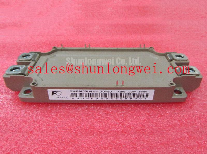
Operating high-capacity power conversion systems (PCS) within utility-scale battery energy storage systems (BESS) installed in mountainous or high-plateau regions exposes power electronics to harsh environmental physics. When equipment runs at elevations exceeding 2000 meters, atmospheric pressure drops while cosmic-ray-induced terrestrial neutron flux rises significantly compared to sea level. For a dual-pack power module like the 2MBI450U4N-120-50 manufactured by Fuji Electric Global Power Semiconductor Technologies, this radiation flux represents a physical mechanism for Single Event Burnout (SEB). High-energy neutrons striking the silicon lattice can trigger localized charge multiplication inside the blocking junction, initiating destructive avalanche breakdown well below the maximum collector-emitter rating of VCES = 1200V (Official Datasheet Specification).
In standard low-altitude plant topologies, a 1200V-rated IGBT operates comfortably with a DC-link voltage between 750V and 850V. At elevations approaching 3000 meters, however, standard terrestrial neutron flux models indicate that operating at sustained high DC voltages multiplies the random failure rate exponentially. To maintain an acceptable target FIT rate (Failures in Time per 109 component operating hours) across multi-megawatt battery energy storage container fleets, engineers must apply strict voltage derating. Derating the continuous DC operating bus voltage down to a window between 650V and 720V (Engineering Calculation based on empirical cosmic ray acceleration factors) cuts the localized peak electric field strength across the drift layer, reducing neutron-triggered catastrophic failure risks by several orders of magnitude.
Transient voltage management across the DC distribution rails requires an equally disciplined layout strategy. Fast switching transients cause voltage spikes caused by high rates of current change through stray circuit loop inductance. Plant maintenance teams dealing with repetitive overvoltage trip codes often discover that physical terminal snubbers have degraded. Installing low-inductance metal oxide varistors (MOVs) coordinated with high-frequency polypropylene film snubber capacitors across the input laminated busbars clips high-frequency inductive kicks before they stress the collector-emitter barrier. When qualifying replacement units or benchmarking operational integrity after unexpected inverter lockouts, reference the diagnostics and fault verification procedures outlined in the Field Engineer’s Handbook to verify module isolation integrity and high-voltage leakage behavior before restoring battery string power.
Baseplate Convexity Compensation and Screw Tightening Sequence Guidelines
Thermal management is the single most critical factor governing long-term mechanical reliability in centralized energy storage inverters running continuous four-quadrant power cycles. The 2MBI450U4N-120-50 is housed in an industry-standard M254 package outline with a physical component weight of approximately 350g (Official Datasheet Specification). The heavy copper baseplate is manufactured with a deliberate, microscopic convex bow. This engineered camber is designed to compress outward during mounting, forcing thermal interface material (TIM) from the center toward the perimeter to eliminate air voids directly beneath the high-heat-density IGBT and freewheeling diode dies.
Applying thermal grease improperly or tightening mounting screws erratically causes baseplate warpage, leading to uneven contact patches, cracked internal direct copper bonded (DCB) ceramic substrates, or thick TIM pockets that act as thermal insulators. To achieve the module's rated collector power dissipation of PC = 2080W (Official Datasheet Specification), the thermal paste layer must be applied using a precision screen printer or a notched squeegee, achieving a uniform wet thickness between 50 µm and 100 µm (General Industry Design Consideration for high-power modules). Applying excess compound leads to hydraulic binding, preventing the copper baseplate from seating directly against the nickel-plated heatsink surface.
Fastening the M254 footprint requires a strict, two-stage torque sequence. The module features four primary chassis mounting holes designed for M5 fasteners. First, hand-tighten all four screws in a diagonal crisscross pattern to approximately 1.0 N·m. Then, apply a final torque of 2.5 to 3.5 N·m (General Industry Design Consideration for M5 chassis mount screws) using a calibrated torque wrench, following the same diagonal path. Allow a settling rest period of at least thirty minutes for high-viscosity silicone-free thermal compounds to flow and expel micro-voids, followed by a final torque verification pass before installing electrical busbars.
Connecting the power terminals requires the same level of discipline. The main collector and emitter busbars use threaded terminals requiring an assembly torque of 3.5 to 4.5 N·m (General Industry Design Consideration for M6 electrical connections). Always install Belleville spring washers beneath flat washers on busbar bolts; solid lock washers fail to compensate for the dynamic expansion and contraction cycles of copper busbars carrying hundreds of amperes. Pay close attention to physical creepage and clearance distances: maintain a minimum of 10 mm through-air clearance and 15 mm surface creepage across exposed power terminations, especially in containerized battery cabinets prone to fine dust infiltration.
⚠️ Maintenance Note: Conduct infrared thermography surveys during full-load charge and discharge cycles on a biannual schedule. A thermal delta greater than 8°C between parallel IGBT module baseplates indicates degraded thermal interface grease, localized voiding, or mechanical torque relaxation. Any module showing excessive thermal differential must be dismounted, the heatsink surface stripped and cleaned with high-purity solvent, and fresh thermal interface material applied at the specified torque.
Dynamic Gate Impedance Control for Robust Phase-Leg Dead-Time Operation
The half-bridge internal topology of the 2MBI450U4N-120-50 switches heavy DC-link voltages across battery racks under continuous pulse-width modulation (PWM). High switching speeds produce steep voltage gradients across the collector-emitter junctions. This fast voltage slew rate injects parasitic displacement currents through the gate-collector Miller capacitance directly into the gate driver output stage. If the impedance of the turn-off gate loop is too high, this induced displacement current develops a voltage bump across the internal gate resistance that can exceed the gate threshold voltage, triggering a momentary cross-conduction shoot-through across the phase leg.
Relying on a 0V turn-off rail to hold the IGBT off during opposing-switch transitions is insufficient in utility-scale conversion hardware. Robust gate driver design demands a negative gate bias between -5V and -15V (Typical Starting Point for bench tuning) combined with a low-impedance active Miller clamp circuit. The active Miller clamp senses the falling edge of the gate voltage; once the gate drops below roughly 2V, an internal low-resistance MOSFET shorts the gate directly to the negative rail, clamping the dynamic impedance below 1.0 Ω. This shunts incoming Miller current away from the gate and prevents parasitic gate re-turn-on.
Dead-time management in firmware must be tuned against hardware turn-on and turn-off delays. For this generation of power silicon, setting an initial hardware dead-time between 2.5 µs and 3.5 µs (Typical Starting Point for bench tuning) provides a reliable safety boundary against overlapping conduction. In auxiliary and control topologies where pre-stage power conversion or active crowbar systems are implemented, system designers frequently pair these main switches with compatible modules such as the 2MBI450UE-120, ensuring consistent turn-off tail times and matching recovery dynamics across interconnected stages.
Bootstrap power supplies operating within high-side gate drive circuits also demand careful component selection. High switching frequencies require bootstrap capacitors with high ripple current ratings and minimal equivalent series resistance (ESR). The bootstrap diode must feature ultra-fast reverse recovery characteristics to block the full DC rail voltage without snapping; snappy reverse recovery creates high-frequency ringing that couples directly into sensitive optocoupler or digital isolator grounds, causing missing PWM pulses or false hardware fault trips.
⚠️ Field Alert: When analyzing gate drive waveforms during inverter commissioning or troubleshooting, never attach an oscilloscope ground lead using an alligator clip. The large loop area captures common-mode radiated EMI and ground bounce, corrupting the real gate-to-emitter waveform display. Always utilize a high-voltage differential probe or connect via an onboard MMCX test jack soldered directly across the auxiliary emitter and gate pins.
Derating Guidelines and Mismatched Parameter Compensation in Parallel Operation
High-capacity battery energy storage converters commonly deploy two or more IGBT modules in parallel per phase leg to scale power throughput. Under standard rating conditions, the 2MBI450U4N-120-50 handles a continuous collector current of IC = 600A at TC = 25°C and IC = 450A at TC = 80°C (Official Datasheet Specification). The typical saturation voltage is VCE(sat) = 2.05V (Official Datasheet Specification), paired with a freewheeling diode forward voltage drop of VF = 1.80V (Official Datasheet Specification). In parallel arrays, slight mismatches in internal saturation voltages or busbar stray inductances cause unequal current sharing between parallel paths.
Fortunately, the trench gate silicon technology used in this module displays a positive temperature coefficient of saturation voltage at elevated current levels. When one module carries a disproportionate share of the load current, its junction temperature rises. As its internal junction approaches the operating limit of Tjop = -40°C to +150°C (Official Datasheet Specification), its saturation voltage increases, which naturally pushes current toward the cooler parallel partner during the on-state period. However, this thermal balancing mechanism cannot counteract dynamic current imbalances that occur during switching transients.
| Operational Condition | Datasheet Baseline | Parallel Fleet Practical Guideline | Engineering Basis |
|---|---|---|---|
| Continuous Current (IC @ 80°C) | 450A | 360A–380A per module | Design Consideration: 15–20% dynamic derating for thermal margin |
| VCE(sat) Tolerance Matching | 2.05V (typical) | Bin matched within ±0.10V | Design Consideration: Prevents steady-state current imbalance |
| Isolation Voltage (1 min) | 2500 VAC | Field proof testing at 1800 VAC max | Design Consideration: Avoids cumulative DCB dielectric stress |
| Gate Resistor Layout | Application dependent | Separate RG per module | Design Consideration: Suppresses parasitic gate-to-gate loop oscillations |
To prevent dynamic current imbalances during turn-on and turn-off, physical symmetrical layout is mandatory. Paralleled modules must feature identical laminated busbar lengths, identical snubber locations, and individual, dedicated gate resistors mounted close to the pins. Paralleling modules through a single, shared gate resistor allows high-frequency circulating currents between the gate terminals, resulting in destructive parasitic oscillation.
When executing field repairs or modular replacements on legacy inverter stacks, engineers may encounter related variants such as the 2MBI450U4N120-50. When evaluating replacements, review mechanical package tolerances, internal thermistor values, and silicon revision suffixes via the Fuji Electric Power Semiconductors Portal. Ensuring identical switching timing and thermal characteristics protects the balanced current distribution required for continuous, reliable power conversion.