Content last revised on February 9, 2026
2MBI200UD-120: An Engineer's Guide to the Fuji 1200V/200A U-Series IGBT Module
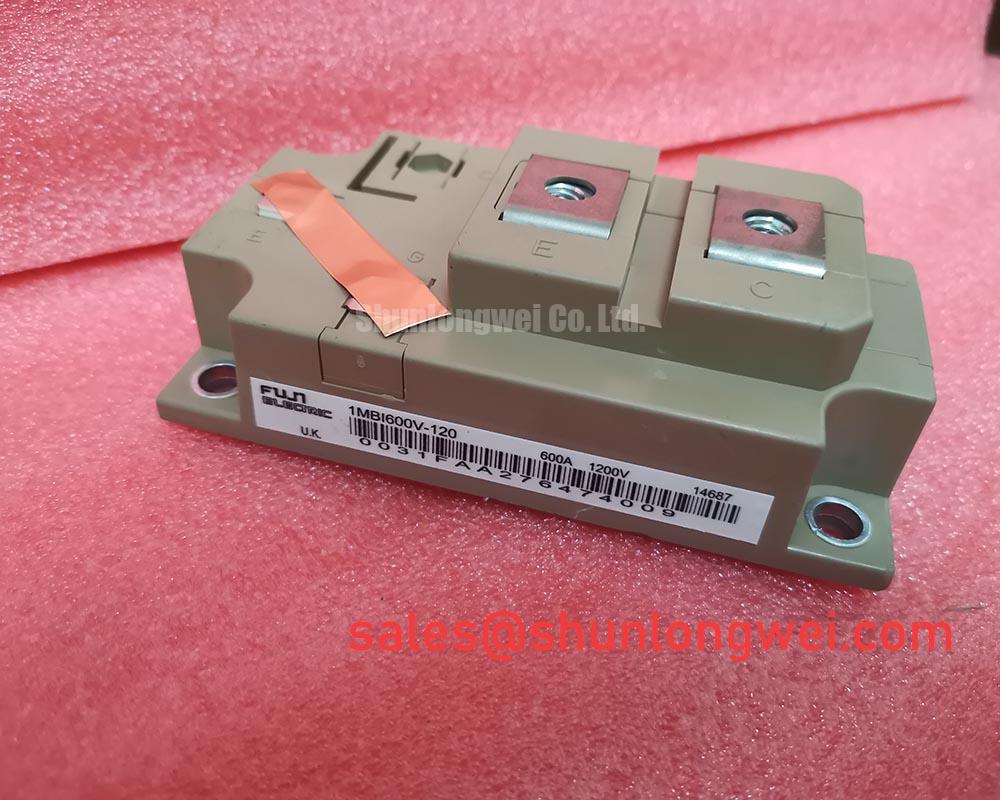
Engineered for demanding power conversion applications, the Fuji Electric 2MBI200UD-120 is a high-performance IGBT module designed to deliver a superior balance of efficiency and switching speed. This device integrates two IGBTs in a half-bridge configuration, rated for 1200V and 200A, with a maximum collector-emitter saturation voltage (VCE(sat)) of 3.2V. Its primary advantages include reduced overall system losses and the ability to operate at higher frequencies, directly supporting the design of more compact and efficient power systems. For high-frequency industrial drives up to approximately 100kW, the 2MBI200UD-120's balance of switching and conduction losses makes it an optimal choice for maximizing system efficiency.
Application Scenarios & Value
Engineering High-Efficiency Inverters and Drives
The 2MBI200UD-120 is particularly well-suited for high-frequency applications where both efficiency and power density are critical design criteria. What is the primary benefit of its U-Series design? Lower losses and higher switching speeds for dense power converters.
In the core of a Variable Frequency Drive (VFD), for example, the fast switching characteristics of this module allow for an increased PWM frequency. This has a direct system-level benefit: it enables the use of smaller, lighter, and more cost-effective inductors and capacitors in the output filter stage, without compromising on motor current ripple or electromagnetic interference (EMI) performance. The module's low VCE(sat) of 2.7V (typical at 125°C) minimizes conduction losses, which is a dominant factor in lower-speed, high-torque motor operation, thereby improving overall drive efficiency across a wider operating range.
This module's capabilities also extend to other demanding applications such as industrial motor controls, Uninterruptible Power Supplies (UPS), and the DC-AC inverter stage of solar power conditioners. For systems requiring higher current handling for more powerful motors, the related 2MBI300HH-120 offers a 300A capability in a similar voltage class. Conversely, for applications built on a 200V or 400V bus architecture, the 2MBI200VA-060 provides a 600V alternative.
Key Parameter Overview
A Data-Centric Look at Switching Performance and Conduction Losses
The performance of the 2MBI200UD-120 is defined by a set of key parameters meticulously engineered for high-frequency power conversion. The values below are extracted from the official datasheet and represent the component's performance under specified test conditions.
| Parameter | Symbol | Value | Conditions | Engineering Significance |
|---|---|---|---|---|
| Collector-Emitter Voltage | Vces | 1200V | - | Provides a robust safety margin for nominal 480V to 600V AC line applications. |
| Continuous Collector Current | Ic | 200A | Tc = 80°C | Defines the module's continuous current handling capability at a typical case temperature. |
| Collector-Emitter Saturation Voltage | VCE(sat) | Typ. 2.7V / Max. 3.2V | Ic = 200A, Tj = 125°C | A primary driver of conduction losses. This low value is akin to low friction, minimizing heat generation during the on-state and boosting overall efficiency. |
| Turn-on Switching Loss | Eon | 27 mJ/pulse | Ic = 200A, Tj = 125°C | Quantifies the energy lost as heat each time the IGBT turns on. Crucial for high-frequency designs. |
| Turn-off Switching Loss | Eoff | 26 mJ/pulse | Ic = 200A, Tj = 125°C | Represents the energy lost during the turn-off event. A balanced Eon/Eoff profile is key to managing thermal loads at high PWM frequencies. |
| Thermal Resistance (Junction-to-Case) | Rth(j-c) | Max. 0.14 °C/W (IGBT) | Per 1/2 Module | Measures how efficiently heat can be transferred from the silicon chip to the module's baseplate, a critical factor in Thermal Management. |
| Forward Voltage (FWD) | Vf | Typ. 2.5V / Max. 3.1V | If = 200A, Tj = 125°C | Dictates the conduction losses in the freewheeling diode, an important factor in inverter efficiency. |
Download the 2MBI200UD-120 datasheet for detailed specifications and performance curves.
Frequently Asked Questions
Practical Insights for Design and Implementation
How do the switching losses (Eon/Eoff) of the 2MBI200UD-120 impact the choice of switching frequency?
The low total switching loss (Eon + Eoff) of approximately 53 mJ per pulse at nominal conditions allows designers to push for higher switching frequencies (e.g., 10-20 kHz) while managing thermal dissipation effectively. This enables the use of smaller magnetics and capacitors, directly contributing to a higher power density. However, total power loss must always be calculated in the context of the target application's specific operating conditions.
What is the significance of the typical VCE(sat) being specified at 125°C?
Specifying VCE(sat) at a high junction temperature of 125°C provides a realistic measure of conduction losses under real-world operating conditions, not just at room temperature. The 2.7V typical value gives engineers a practical number for calculating thermal performance and efficiency when the module is running under load, which is essential for accurate system design as detailed in many datasheets.
Is this module suitable for paralleling to achieve higher current output?
While the datasheet does not explicitly detail paralleling procedures, it is a common practice in power electronics. Successful paralleling requires careful attention to symmetrical layout to ensure balanced current sharing, as well as considering the positive temperature coefficient of VCE(sat), which helps naturally balance current between parallel devices. A gate drive circuit designed with this in mind is critical.
Technical Deep Dive
Inside the U-Series: How Low Internal Inductance Maximizes Switching Performance
One of the defining features of the 2MBI200UD-120 is its "low inductance module structure," a design element that is crucial for unlocking its high-speed switching potential. In any power module, parasitic inductance exists in the internal connections between the terminals and the semiconductor die. During fast switching, particularly at turn-off, this inductance can cause significant voltage overshoots (Vce spikes) due to the rapid change in current (L*di/dt).
Think of this internal inductance like a long, coiled fire hose. If you shut the nozzle off abruptly, a powerful pressure wave, or "water hammer," surges back through the hose. In an IGBT module, this "water hammer" is a voltage spike that can exceed the device's 1200V breakdown rating, leading to degradation or immediate failure.
The U-Series design minimizes this effect by using an optimized internal layout with wide, flat conductors and symmetrical placement to reduce the length and area of current loops. This is analogous to replacing the long, coiled hose with a short, wide, and straight pipe. The result is significantly lower parasitic inductance. For a design engineer, this translates into several tangible benefits:
- Enhanced Reliability: Reduced voltage stress on the IGBT die during every switching cycle leads to a longer operational lifespan.
- Cleaner Switching: Lower overshoot minimizes ringing and electromagnetic interference (EMI), potentially reducing the need for complex and lossy snubber circuits.
- Faster Performance: With overshoot well-controlled, the IGBT can be switched off more aggressively, enabling higher frequency operation and further improving power density.
This focus on minimizing internal inductance is a key enabler, allowing systems to harness the full speed of the silicon without compromising the Safe Operating Area (SOA) of the device.
Strategically leveraging a module like the 2MBI200UD-120 allows engineering teams to move beyond incremental efficiency gains and architect next-generation power converters that are fundamentally more compact, reliable, and cost-effective. Its balanced loss profile and high-speed-enabling structure provide a critical building block for meeting aggressive power density and performance targets in modern industrial systems.