Content last revised on September 10, 2026
Preventing Spurious Faults: Mitigating Hard Switching Transients via A Guidelines for 2MBI200VH-120-50
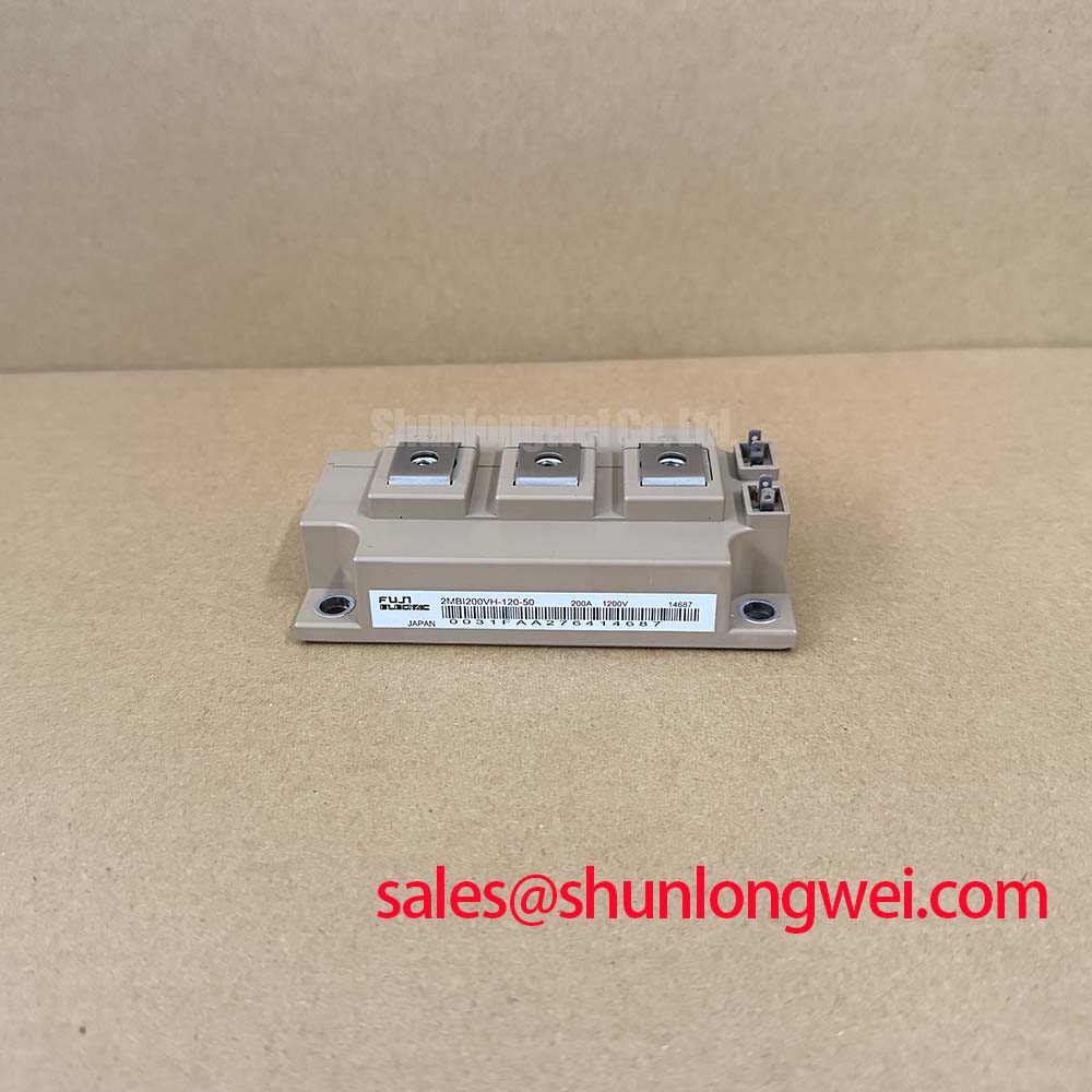
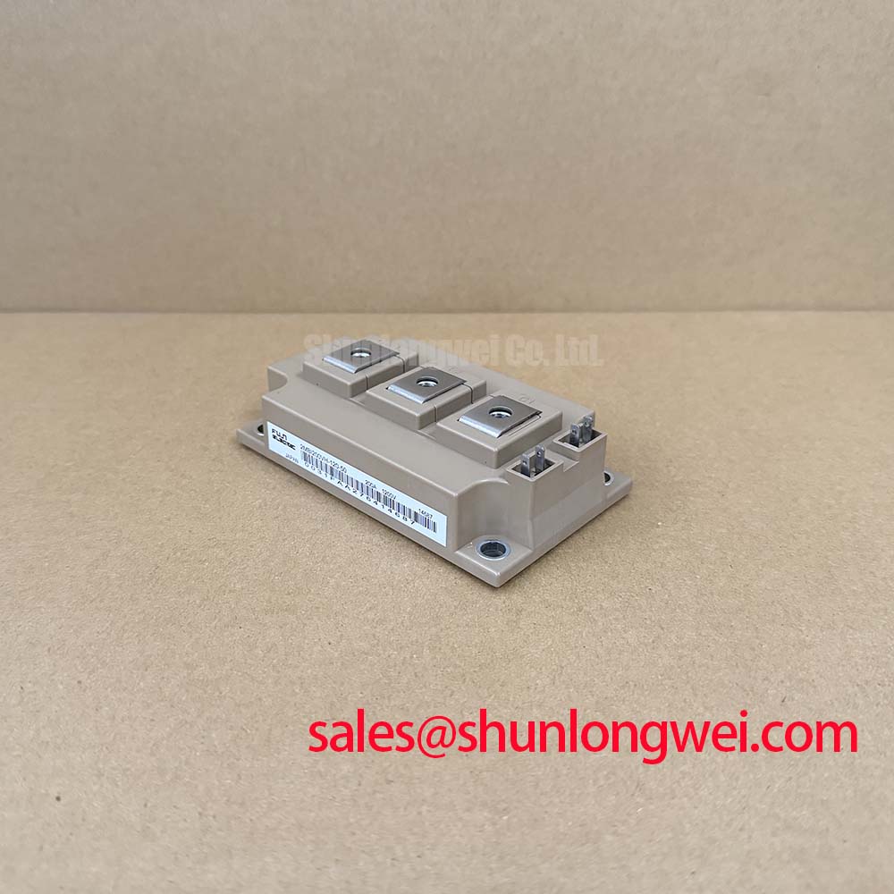
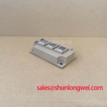
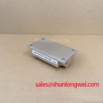
Before mounting a replacement 2MBI200VH-120-50 dual-pack module into a downed commercial string inverter or energy storage power conversion system, verify collector-to-emitter cold resistance across both switches using a calibrated digital multimeter. The Fuji Electric 2MBI200VH-120-50 is rated for a maximum collector-emitter voltage of 1200 V (VCES) and a continuous collector current of 200 A at a case temperature of 100°C (reaching 240 A at 25°C). When troubleshooting severe switching faults in high-capacity string topologies, engineers must address short-circuit safe operating area (SCSOA) limitations. Under severe load short-circuits (Type-I) or bus shoot-through events (Type-II), fault current escalates rapidly, necessitating desaturation detection and active gate suppression within 10 microseconds to prevent silicon fracture.
Hard turn-off under fault currents exceeding three times the nominal 200 A rating induces destructive collector-emitter inductive voltage spikes. To safeguard the 1200 V physical breakdown boundary, gate drive designs should incorporate two-stage soft turn-off (2SSTO). When desaturation circuitry detects a threshold breach (typically calibrated around 6.5V to 7.5V VCE sensing threshold), the driver clamps gate-emitter voltage from +15V down to an intermediate 7V to 8V plateau for roughly 1.5 to 2.5 microseconds before pulling it fully to -8V. This stepwise reduction suppresses current fall velocity (di/dt), keeping transient voltages well below the 1200 V physical breakdown threshold without causing catastrophic punch-through failure.
Assembly Integrity & Layout Architecture: Implementing Optocoupler vs Digital Coreless Transforme for 2MBI200VH-120-50
Decoupling high-voltage bus transients from sensitive digital signal processing circuitry demands strict isolation integrity across the inverter bridge. The 2MBI200VH-120-50 package provides an isolation rating of 4000 V AC for 1 minute between terminals and baseplate, yet driver isolation must maintain reinforced galvanic barriers exceeding 5 kV to guarantee system-level safety. While traditional optocouplers historically served gate transmission, their LED performance degrades over decades of thermal cycling, causing propagation delay drift. Modern micro-grid storage converters increasingly implement digital coreless transformer isolators or capacitive isolation ICs capable of delivering common-mode transient immunity (CMTI) exceeding 100 kV/µs.
In high-speed switching loops where dv/dt exceeds 15 kV/µs, insufficient CMTI allows displacement currents to traverse isolation barrier capacitance, generating false gate trigger pulses that cause simultaneous top- and bottom-switch conduction. Complementary fast-recovery freewheeling diodes within the module present a junction-to-case thermal resistance Rth(j-c) of 0.200 °C/W, while the IGBT silicon delivers an Rth(j-c) of 0.135 °C/W. When high-frequency pulse-width modulation interacts with grid-tied inductive chokes, layout engineers must route primary and secondary driver traces orthogonally across internal PCB ground planes to prevent capacitive cross-coupling. For comprehensive structural comparisons of planar power architectures, technicians can explore technical references from Shindengen Power Semiconductor Modules & Diodes alongside modern packaging topologies from Fuji Electric 7th-Gen X-Series IGBT Modules.
Assembly Integrity & Layout Architecture: Implementing Calculating Failures-in-Time Rates in Hig for 2MBI200VH-120-50
Deploying string inverters and containerized micro-grid energy storage platforms at high altitudes (exceeding 2000 meters above sea level) introduces operational hazards associated with atmospheric cosmic radiation. Atmospheric secondary neutron flux escalates exponentially with elevation, dramatically increasing the probability of Single Event Burnout (SEB) within the high-field drift region of the silicon. While the 2MBI200VH-120-50 specifies an absolute maximum VCES of 1200 V and allowable operating junction temperature (Tjop) up to 150 °C, running steady-state DC bus voltages near the physical rating at elevated altitude drives Failure-in-Time (FIT) rates into unacceptable territory.
As an established engineering design consideration, keeping nominal DC-bus operating voltage derated to 800V–850V maintains cosmic radiation-induced FIT rates within industrial mission-profile boundaries. Field technicians replacing damaged power stages in high-altitude solar farms must assess whether recurring module failures stem from cosmic-ray avalanche degradation rather than simple over-temperature events. When system upgrades require elevated thermal margin or continuous power capacity expansion beyond 200 A, technicians often evaluate drop-in physical footprints such as the 2MBI300U4H-120-50 dual module to reduce relative current loading per square millimeter of die area. Deep technical fundamentals governing drift region avalanche breakdown and carrier dynamics are detailed in The Ultimate IGBT Knowledge Base.
2MBI200VH-120-50 Operational Boundaries: Evaluating High-Frequency Commutation Loop Inductance Limits
During hard commutation in utility-scale string inverters, collector current extinguishes at rates often exceeding 2000 A/µs. The resulting peak turn-off voltage corresponds directly to the sum of the DC link bus voltage and the product of parasitic commutation loop inductance multiplied by current fall velocity, expressed continuously in circuit operation as peak collector-emitter voltage equals DC link voltage plus stray inductance multiplied by di/dt. With a maximum collector dissipation rating of 1110 W per switch and typical terminal saturation voltage VCE(sat) of 1.95 V (maximum 2.40 V at 200 A, 25°C), mitigating transient turn-off voltage overshoot preserves both electrical insulation and thermal headroom.
⚠️ Field Alert: When seating the module against the cast aluminum or copper heatsink, apply an even, non-silicone thermal interface layer between 50 and 80 microns thick across the baseplate. Fasten the M5 mounting bolts diagonally in a crosswise two-step pattern, first hand-tightening to approximately 1.0 N·m, followed by final torque between 2.5 and 3.5 N·m. Excessive torque warps the internal ceramic substrate, whereas under-torque elevates thermal impedance above the factory maximum 0.135 °C/W junction-to-case threshold, precipitating junction thermal runaway.
To restrict total loop inductance (L_sigma) below 25 nH, power stage designers employ wide, low-profile laminated busbars where positive and negative DC conductors run parallel with thin polyimide dielectric insulation. Paralleling low-inductance polypropylene snubber film capacitors directly across the module collector and emitter terminals absorbs high-frequency inductive energy during reverse recovery. Verifying planar busbar bolt torque, snubber capacitance balance, and gate resistor damping on the workbench ensures that the 2MBI200VH-120-50 operates securely within its dynamic safe operating area across demanding solar and battery cycling regimes.