
Content last revised on September 19, 2026
PM75CS1E120 Inspection and Benchtop Waveform Tuning: Mitigating Stress via PCB Symmetry Considerations for the IGBT Module
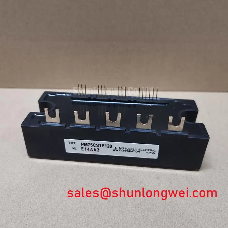
Before powering a drive, isolate the DC link, inspect the module housing and terminals for mechanical damage or heat evidence, then verify that the nameplate matches PM75CS1E120, Mitsubishi Electric, 1200 V, and 75 A. These are Official Datasheet Specifications for a Mitsubishi IPM Module; terminal functions, driver connections, protection behavior, and operating limits must be confirmed against the original equipment documentation and the applicable Mitsubishi Electric technical documentation.
| Parameter | Value | Classification |
|---|---|---|
| Product model | PM75CS1E120 | Official identification |
| Manufacturer | Mitsubishi Electric | Official identification |
| Voltage rating | 1200 V | Official Datasheet Specification |
| Current rating | 75 A | Official Datasheet Specification |
| Package category | Mitsubishi IPM Module | Official package classification |
For a heavy-duty variable frequency AC motor drive, these ratings establish the initial electrical boundary only. A repair decision also depends on the original gate-drive arrangement, control-board interlock behavior, cooling assembly, DC-link condition, motor cable arrangement, switching waveform, and the actual terminal pattern in the equipment. Mitsubishi Electric publishes its power semiconductor portfolio and technical resources through its Power Semiconductors and High-Power Modules information center.
Start with the drive board disconnected from the power stage where the equipment architecture permits it. Compare the gate-drive outputs, isolated supply rails, command paths, and interlock signals between corresponding inverter channels. A static resistance check can reveal a hard short or a damaged gate-drive path, but it cannot prove correct switching behavior. Before fitting a replacement PM75CS1E120, inspect the mating busbar faces, terminal hardware, connector seating, and signs that a previous event has displaced or overheated surrounding parts.
Design Consideration: high-current emitter return paths and low-level gate-drive returns should not share an uncontrolled section of conductor. During a switching transition, current in the power loop can create a voltage shift in a shared return path. The gate driver then sees a gate-to-emitter voltage different from the voltage expected by the controller. That difference can appear as ringing, erratic turn-on, reduced turn-off authority, or unequal behavior between switching positions.
Where the equipment provides a separate auxiliary emitter or driver-return connection, keep its route dedicated to the gate driver and separate it from the main load-current return. This is a PCB and interconnection symmetry issue rather than a generic wiring preference. The objective is to minimize common impedance between the gate-drive reference and the main switching-current path, especially where turn-off overshoot must be controlled. The system engineer should verify the resulting gate-to-emitter waveform directly at the relevant module connection while checking peak collector-emitter voltage against the DC-link operating condition.
For field work, inspect whether replacement leads have been extended, rerouted, bundled with power conductors, or terminated under the same hardware as high-current returns. Such changes can alter the original switching loop even when continuity checks pass. If oscillation is suspected, compare the affected drive channel with a known-good channel using suitably rated isolated measurement equipment. Observe command timing, gate-emitter behavior, DC-link disturbance, and phase-current response together. A single noisy waveform does not identify one root cause; poor probing practice, a degraded driver supply, loose power hardware, or an altered return path can produce similar symptoms.
When an installed part cannot be restored and an alternative is being evaluated, the SKIIP37AC12T4V1 can be reviewed as a separate module option. It should not be treated as a direct substitution based on voltage or current markings alone. The system integrator should compare terminal assignment, package dimensions, mounting interface, gate-drive requirements, protection interfaces, thermal path, and the complete drive topology before determining whether it is suitable for a particular repair.
Field Alert: Tighten power and mounting hardware only to the torque specified for the original equipment hardware, and apply thermal interface material as a uniform thin layer before final assembly.
PM75CS1E120 Thermal-Electrical Optimization: Suppressing Cres-Induced Gate Voltage Spike Practical Tuning
A motor drive can show a gate-voltage disturbance even when the controller command is held off. Fast collector-emitter voltage movement transfers charge through the device capacitances into the gate circuit. If the off-state gate path has excessive impedance or its reference moves with switching current, the induced gate excursion can become significant enough to disturb the intended off state. In a bridge leg, this can create concern about cross-conduction, particularly when the complementary device is switching under load.
Design Consideration: evaluate the complete off-state gate path, including the driver output stage, turn-off resistor network, return trace, isolation barrier arrangement, and any gate clamp provided by the original design. A dedicated low-impedance active Miller clamp can hold the gate closer to its emitter during high collector-voltage slew conditions when that feature is supported by the gate driver. A negative gate bias is also commonly evaluated where the original system architecture and module documentation allow it. The final bias arrangement is system-determined and must be verified against the gate-emitter absolute maximum ratings, the driver supply capability, and measured switching behavior.
Do not add a negative supply, clamp circuit, or revised gate resistance as an unverified repair shortcut. Changes that improve apparent immunity on one channel can increase switching loss, alter protection timing, or create an asymmetry between bridge positions. An Engineering Recommendation is to preserve the original drive architecture first, then investigate deviations only through controlled bench testing with appropriate protection and measurement methods.
High-side gate-power integrity requires the same discipline. In bootstrap-supplied designs, capacitor selection must account for the documented gate charge of the controlled switch, driver quiescent current, switching interval, leakage paths, permitted bootstrap-voltage variation, and the actual modulation pattern. The gate charge value for PM75CS1E120 should be taken from the applicable official documentation rather than inferred from the 75 A rating. A capacitor that appears adequate at light load can lose effective gate drive under a waveform or duty condition that leaves insufficient refresh time.
During diagnosis, verify that the high-side drive supply is refreshed through the intended switching cycle and that the gate driver has not entered an undervoltage or fault state. Examine the local drive supply at the driver pins with a measurement method that does not create a false ground path. A gate waveform with a depressed plateau may indicate several possible conditions, including supply weakness, a protection response, excessive impedance, or a measurement reference problem. Compare it with the known-good signal path before replacing the IPM.
The 1200 V rating is an Official Datasheet Specification, not a statement that every DC-link transient in an existing drive is acceptable. Design Consideration: minimize the commutation-loop inductance to suppress turn-off inductive overshoot, then verify peak voltage margin during switching tests under the equipment’s actual operating conditions. Practical gate-drive, thermal-interface, and topology checks are collected in this IGBT Design & Integration technical reference.
Transient Dynamics & Electrical Design: Transient Thermal Impedance on PM75CS1E120
After a drive trip or intermittent thermal fault, first inspect the heatsink contact region and cooling path before drawing conclusions from a surface temperature reading. Check that the heatsink is clean, the module sits flat, mounting hardware is present, cooling fans or liquid-flow hardware operate as intended, and the thermal interface has not been displaced. A localized heat mark near one connection can also point toward high-resistance electrical hardware rather than a semiconductor failure.
The steady-state thermal path and the pulsed thermal path are different engineering questions. A transient thermal impedance curve, when provided in official documentation, describes how junction-to-case temperature response develops during a pulse and subsequent cooling interval. For repeated overloads, the relevant calculation uses the manufacturer’s transient thermal model or curve, the measured or calculated loss profile, pulse duration, repetition behavior, case temperature, and the permitted junction-temperature boundary. This is an Engineering Calculation only when based on those documented inputs; it must not be replaced with a generic temperature estimate.
For a heavy-duty variable frequency AC motor drive, acceleration, stalled-load protection events, rapid speed changes, and braking transitions can create a loss pattern unlike nominal continuous operation. The repair engineer should establish whether the event occurs during switching, conduction, regeneration, or a cooling-system change. Current trend data, drive fault history, phase balance, DC-link behavior, and thermal imaging can help narrow the test plan. They do not independently establish junction temperature or module remaining life.
Design Consideration: use the module’s official transient thermal information, if available for the exact product, rather than applying a thermal curve from another package. Package construction, die arrangement, baseplate interface, and thermal network behavior are product-specific. The Mitsubishi IPM Module package designation alone does not supply enough information to calculate thermal margins for a particular pulse.
Where the original controller provides desaturation, overcurrent, or soft-turn-off protection, verify the protection sequence before returning the drive to service. A protection response can prevent a destructive event, but only if the sensing network, gate-drive supply, logic interlock, and fault reporting path remain intact. Inspect the driver board for damaged sensing resistors, isolation components, connectors, and power-supply rails. A module replacement without this inspection can leave the initiating fault in place.
There is no basis here for assigning a service-life value, a failure rate, a cosmic-ray susceptibility value, a high-altitude derating factor, or an insulation qualification to this specific module. Where the equipment operates outside its documented environmental envelope, system-level qualification and manufacturer documentation are required. The repair focus should remain on measured electrical stress, cooling effectiveness, mechanical assembly, and the original protection behavior.
PM75CS1E120 Operational Boundaries: Evaluating Dynamic Braking Chopper Operation Limits
When a variable frequency drive faults during deceleration, determine whether the DC-link voltage rises only while the motor is returning energy to the drive. This observation can direct attention toward the braking chopper circuit, braking resistor assembly, control enable path, DC-link capacitance condition, or the mechanical load profile. It does not prove that the IPM is responsible. Isolate and test the relevant circuit according to the equipment service procedure before reconnecting the motor and applying power.
A braking system converts kinetic energy from decelerating equipment into heat, commonly through a controlled chopper path and a braking resistor. The energy requirement depends on motor and load inertia, speed change, deceleration time, repeated-cycle behavior, the DC-link operating point, and the resistor’s thermal capacity. The chopper semiconductor and resistor must therefore be assessed as a system. The PM75CS1E120 voltage and current ratings cannot alone establish braking-chopper suitability, whether an internal function exists, or whether an external chopper is correctly dimensioned.
Engineering Recommendation: verify the original schematic to identify whether braking control is implemented through a separate transistor, a dedicated power module, or another arrangement. Confirm the resistor value and duty capability from the equipment documentation, inspect its wiring and thermal protection, and check that the controller commands braking only under the intended conditions. A failed resistor connection, a damaged chopper driver, or a DC-link sensing fault can each lead to overvoltage behavior during deceleration.
For a repair bench, begin with a controlled operating condition and capture DC-link voltage, speed command, actual speed, braking command, and fault indication using equipment-appropriate instrumentation. Increase operating demand only under the original protection system and within the machine’s documented procedure. Watch for abnormal rise in DC-link voltage, missing braking command, unexpected trip timing, or unequal phase behavior. The system engineer should then determine whether the electrical and thermal limits remain acceptable for the actual braking cycle.
In the wider drive power chain, a module such as BSM75GD120DLC can be examined as a related power-stage component where the original topology uses a separate switching function. Its presence in a comparison list does not establish interchangeability with PM75CS1E120. Confirm the role in the circuit, electrical ratings, pinout, insulation and mounting requirements, drive interface, and protection coordination against the original equipment design.