

Content last revised on October 10, 2026
Assembly Integrity & Layout Architecture: Implementing Suppressing Cres-Induced Gate Voltage Spikes for 2MBI300F-060
Control the gate loop and the power commutation loop as separate physical current paths. During a fast collector-voltage transition, capacitive coupling through device and layout capacitances can move the inactive gate potential. If that induced gate voltage reaches the turn-on region while the complementary switch is conducting, cross-conduction and shoot-through can occur. The practical objective is to reduce the coupling path, provide a low-impedance gate return, and let the driver actively control the off-state gate.
Use the shortest practical connection between the driver output, gate terminal, and emitter return. The gate resistor, damping components, and any active Miller-clamp connection should be placed according to the driver topology rather than distributed across a long control harness. Keep the gate loop away from the collector and DC-link switching paths. A compact layout reduces the opportunity for the switching node to inject current into the control loop, while a clearly defined reference point prevents the driver from sensing a voltage created by power-current sharing.
An active Miller clamp can be considered when the driver supports it and when the measured turn-off waveform shows unwanted gate movement during the opposing switch transition. A negative off-state gate bias can also be evaluated in systems designed for that operating method, but the selected value must come from the driver, module, insulation, and transient-voltage assessment. It should not be copied from an unrelated IGBT family. Verify the gate-emitter voltage directly at the module terminals with suitable probing technique, not only at the driver-board connector.
For a heavy-duty variable-frequency AC motor drive, the braking chopper deserves the same layout discipline as the motor inverter legs. The chopper current path, braking resistor connection, and DC-link return can create a high-energy commutation loop. Minimize its parasitic inductance by arranging the conductors with a controlled return path, then verify turn-off overshoot during a controlled switching test. The peak voltage must remain within the system’s validated semiconductor and insulation boundaries under the actual DC-link and braking conditions.
When a gate waveform shows ringing, first separate driver instability from power-loop coupling. Compare the waveform at the driver output and directly at the module gate-emitter terminals. Check the gate-return conductor, clamp connection, driver supply decoupling, and switching-node probe placement. If the disturbance changes when the power bus is physically repositioned, the result points toward layout coupling rather than a simple gate-resistor value problem. Any corrective damping should be treated as a Typical Starting Point and confirmed with switching measurements.
The Fuji Electric V-Series IGBT Application Manual provides useful manufacturer-level guidance on gate driving, switching behavior, protection, and application evaluation. Use it as a technical reference while matching the actual gate terminal arrangement and ratings for the installed module.
Benchtop Waveform Tuning: Mitigating Stress via Terminal Screw Engagement Depth on 2MBI300F-060
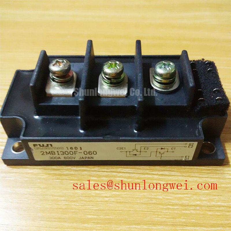
Mechanical installation affects electrical reliability because the main terminal screws transfer clamping force into the module terminals and connected busbars. Excessive screw engagement, an unsuitable washer stack, or a busbar that does not sit naturally on the terminal can introduce levering force into the internal joints. That stress can become more severe during vibration and thermal cycling, even when the first power-up appears normal.
Before tightening, place the busbar over the terminal and confirm that it contacts evenly without being pulled into position by the screw. The screw should engage the available threaded depth without bottoming against the internal terminal structure. Use the fastener, washer arrangement, and torque procedure specified for the actual mechanical assembly. Do not transfer a torque value from another Fuji module simply because the housings look similar.
💡 Bench Tip: De-energize and discharge the power stage before inserting or removing gate and auxiliary wiring, then record the cold-state terminal measurements for comparison after assembly.
Thermal interface preparation also matters. The heatsink surface should be clean, flat, and free from particles that can tilt the baseplate or create a local pressure point. Apply the selected thermal interface material in a controlled, even manner and tighten the mounting hardware in a sequence that keeps the module seated. The correct mechanical procedure is system-specific; the manufacturer’s mechanical drawing and assembly guidance take priority over general workshop practice.
Parallel power modules require symmetrical electrical and thermal conditions. A busbar layout with similar current-path geometry helps reduce unequal stray inductance, while matched cooling conditions reduce temperature imbalance. IGBT conduction voltage typically changes with temperature, so the observed current sharing is influenced by junction temperature, gate timing, busbar resistance, and dynamic switching behavior. Do not judge parallel sharing from one low-current static reading. Use phase-current measurements and thermal observation under the intended operating sequence.
Regenerative braking adds a separate energy-management concern. When motor energy raises the DC-link voltage, the braking chopper must direct that energy to the resistor without exceeding the switching device’s validated voltage and thermal boundaries. Inspect the braking resistor connections, chopper command timing, fuse coordination, and DC-link sensing path together. A failed resistor, open connection, or delayed command can expose the power stage to an abnormal transient even when the inverter output waveform is otherwise correct.
Fast freewheel diodes influence commutation stress and conducted as well as radiated interference. Reverse-recovery softness, recovery current, stray inductance, and gate timing interact during the transition. Avoid assigning a soft-recovery factor to this specific module unless it is explicitly documented for the exact device and test condition. Instead, observe the diode-current and switch-voltage waveforms with a properly compensated differential probe and compare them against the approved design test limits.
Protection coordination should include the semiconductor fuse, DC-link protection, gate-driver desaturation or overcurrent response, and the mechanical condition of the power path. Fuse selection requires coordination with the system short-circuit energy and the module’s documented short-circuit capability; an I2t value taken from a generic fuse table is not sufficient by itself. The protection response must be tested with the complete gate-drive and bus structure, not inferred from a static continuity check.
The manufacturer’s Fuji Electric PIM and power module reference information can help engineers distinguish package-level application considerations from the ratings of a particular circuit configuration. For replacement work, preserve the original terminal function and mounting geometry unless the redesigned assembly has been validated independently.
2MBI300F-060 Operational Boundaries: Evaluating Auxiliary Emitter Return Trace Separation Limits
Keep the gate-driver emitter return separate from the high-current emitter path until the intended reference point. When both currents share a narrow conductor, the voltage generated by power-current change can appear in the gate signal. The driver may then receive a distorted reference, producing apparent gate ringing, unequal turn-off behavior, or unstable current sharing between parallel paths.
Route the auxiliary emitter return as a dedicated low-inductance control trace or conductor, following the module terminal arrangement specified by the applicable drawing. Do not allow it to run alongside the collector busbar for unnecessary distance. Where the control return must cross a power conductor, use a layout arrangement that minimizes mutual coupling and keeps the crossing controlled. The required clearance and separation are determined by the insulation system, voltage environment, contamination level, and mechanical construction; the designer must verify those conditions in the completed assembly.
During troubleshooting, compare three points: the driver reference, the auxiliary emitter terminal, and the main power emitter connection. A differential measurement between the auxiliary and power emitter paths can reveal whether the control reference is moving during switching. If the disturbance appears only when load current rises, inspect shared copper, connector pins, busbar joints, and mounting interfaces before changing gate-drive parameters.
Parallel modules make emitter-return routing especially sensitive. Each gate driver should see a consistent local reference, and the power bus should present similar current-path geometry to each module. Avoid combining several auxiliary returns at a remote controller board if that arrangement forces switching current through the control reference. When a redesign is unavoidable, validate the gate-emitter waveform for every parallel position rather than measuring only the physically nearest device.
The same separation principle applies to a braking chopper. Its emitter return, gate loop, and resistor-current path should be reviewed as a complete commutation network. The braking resistor absorbs regenerated energy, but its switching current can still disturb the driver reference through shared inductance. Verify the chopper gate signal during acceleration, deceleration, and fault interruption, paying attention to the transition where the DC-link voltage changes most rapidly.
For engineers comparing related service parts, the 2MBI150NC-060-10 is a separate Fuji Electric module that should be assessed by its own voltage, current, terminal, thermal, and switching data rather than treated as an automatic substitute. In the upstream power path, the 6MBI30FA-060 may appear as a related module in some equipment architectures, but compatibility depends on the actual rectifier, inverter, control, and protection topology.
When evaluating longer service operation, record the gate-emitter waveform, collector-emitter overshoot, phase-current balance, heatsink temperature distribution, and fault response under controlled conditions. Do not use a single static diode-test result to predict field lifetime. For topology-level background on resonant and half-bridge energy paths, consult Resonant Topologies in Home Appliances and relate its discussion to the actual industrial drive schematic rather than assuming that every topology applies to this module.