Content last revised on October 24, 2026
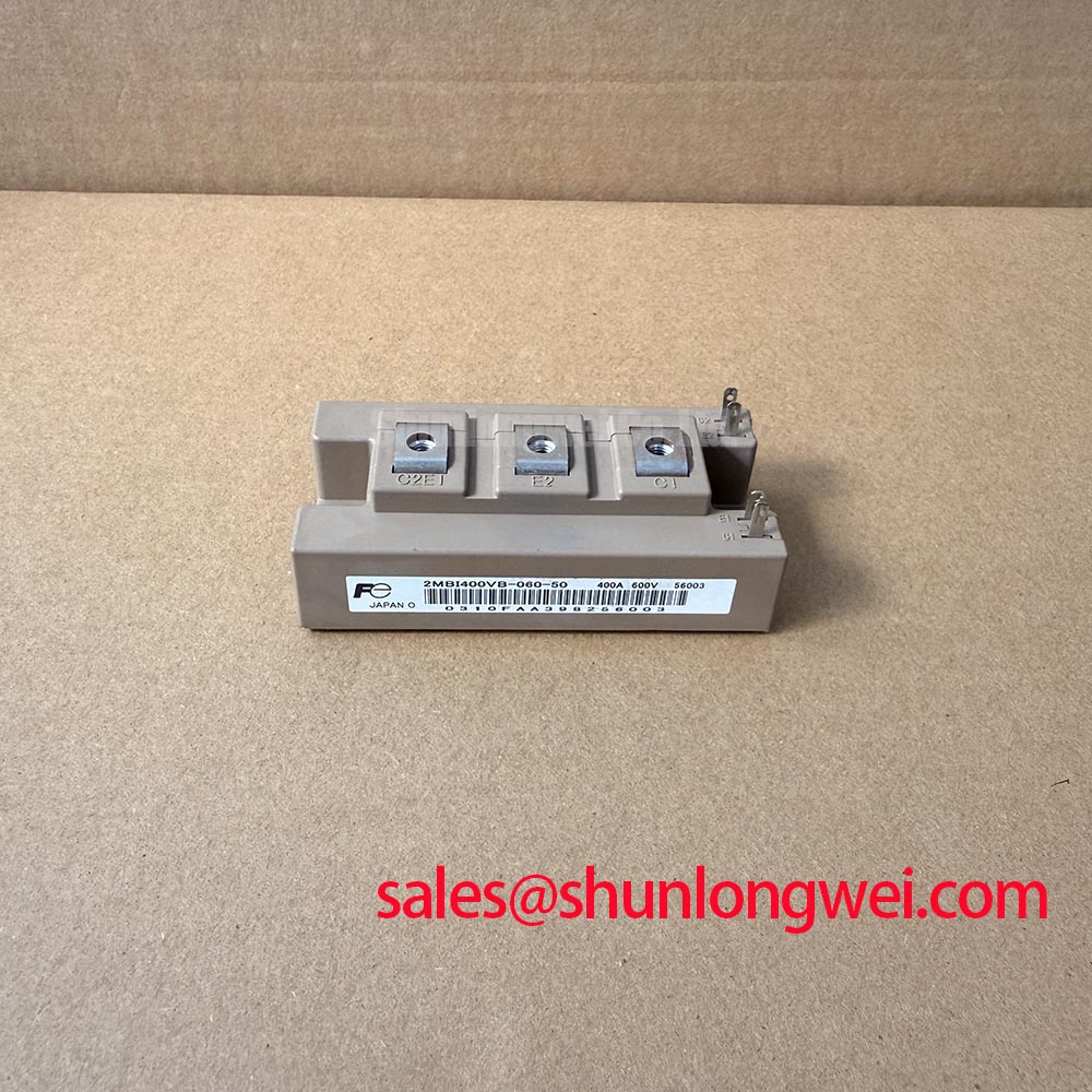
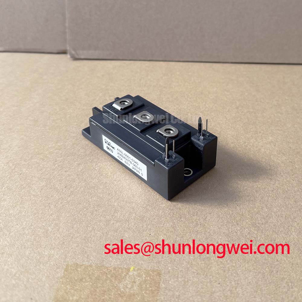
2MBI400N-060-01 Fuji Electric 600V 400A IGBT Module
- Measure cold-state impedance across the main power terminals before connecting the DC link.
- Inspect the baseplate, terminal threads, insulating hardware, and heatsink contact surface for mechanical damage.
- Confirm gate-drive isolation and the correct gate-emitter reference before applying control power.
- Compare the installed module’s voltage and current ratings with the converter’s measured operating envelope.
The Fuji Electric 2MBI400N-060-01 is a high-current IGBT module rated at 600 V VCES, with a continuous collector current of 400 A at Tc = 80°C. Its electrical limits make it a candidate for evaluation in high-power switching equipment, including centralized battery energy storage power conversion systems, subject to the complete converter topology, cooling arrangement, switching conditions, and protection design.
| Parameter | Symbol | Test Condition | Official Specification |
|---|---|---|---|
| Collector-emitter voltage | VCES | Not specified | 600 V |
| Gate-emitter voltage | VGES | Not specified | ±20 V |
| Continuous collector current | IC | Tc = 80°C | 400 A |
| Pulsed collector current | ICP | 1 ms pulse | 800 A |
| Maximum power dissipation | PC | Not specified | 1650 W |
| Collector-emitter saturation voltage | VCE(sat) | IC = 400 A, VGE = 15 V | 2.2 V typical, 2.8 V maximum |
| Gate-emitter threshold voltage | VGE(th) | IC = 400 mA, VCE = 10 V | 5.5 V minimum, 7.5 V maximum |
| Junction-to-case thermal resistance, IGBT | Rth(j-c) | Per IGBT | 0.085 °C/W |
| Junction-to-case thermal resistance, diode | Rth(j-c) | Per diode | 0.15 °C/W |
| Maximum junction temperature | Tj | Not specified | +150°C |
Transient Dynamics and Electrical Design for Bi-Directional DC-DC Buck-Boost Conversion
In a bidirectional battery energy storage converter, current changes direction as the system alternates between battery charging and DC-link support. The switching bridge must therefore be assessed in both power-flow directions rather than only under battery discharge. The 2MBI400N-060-01 provides a 600 V collector-emitter rating and a 400 A continuous collector-current rating under the stated case-temperature condition, but the usable operating point remains dependent on junction temperature, switching frequency, conduction loss, transient overshoot, and the thermal assembly.
During commissioning, record the gate-emitter waveform at the module terminals rather than at the distant driver output. Gate-loop parasitic inductance can create ringing, false turn-on, or uneven parallel-device switching. A practical design consideration is to keep the gate-drive return physically associated with its corresponding emitter path and to separate power commutation conductors from sensitive control wiring. If the assembly provides an auxiliary emitter connection, the system designer should verify its terminal definition and route it independently from the high-current emitter path where the driver reference requires that arrangement.
For a centralized battery energy storage PCS, the DC-link loop, switching bridge, snubber or clamping network, and battery-side inductor must be evaluated as one commutation system. MOV selection is a system design consideration rather than a module specification. Its voltage rating, energy capability, ageing behavior, and coordination with any active clamp should be verified against measured switching transients. The objective is to control collector-emitter overshoot without allowing the protection network to conduct unnecessarily during normal operation.
When a converter trips during high-rate peak shaving, compare the gate waveform, collector-emitter waveform, DC-link voltage, and phase current at the same time base. A current imbalance may arise from gate-loop impedance, unequal conductor inductance, sensor timing, or thermal differences. The diagnostic decision should follow the measured signal path instead of assigning the fault to the IGBT module alone. Fuji Electric’s general semiconductor information can be reviewed through the Fuji Electric 7th-Gen X-Series IGBT Modules resource for broader switching technology context.
Failure-in-Time and High-Altitude Design Considerations
Terrestrial neutron exposure and altitude-related environmental conditions require a documented reliability assessment when a PCS is installed at elevated altitude. A specific FIT or Single Event Burnout rate cannot be assigned to this module from its electrical rating table alone. Such a calculation requires an authoritative device test method, neutron spectrum, geographic exposure model, DC-bus operating distribution, and failure criterion. The system reliability engineer should use qualified manufacturer or standards-based data before converting exposure into a FIT estimate.
The practical field task is to establish the actual voltage stress seen by the collector-emitter terminals during switching, including turn-off overshoot and regenerative events. The 600 V VCES rating is an official device limit, not a permission to operate a converter at an assumed fixed DC-bus value under every altitude and transient condition. Designers should define voltage headroom from measured worst-case switching behavior and the applicable environmental derating policy, then verify it during controlled switching tests.
Thermal interface preparation remains important because the official junction-to-case thermal resistance is 0.085 °C/W per IGBT and 0.15 °C/W per diode. These values describe the semiconductor-to-case path; they do not include thermal compound, mounting flatness, heatsink resistance, airflow, or cabinet temperature. As a general design consideration, a thin and continuous TIM layer is preferred, with the commonly used 50–80 µm range treated as an assembly starting point rather than a Fuji Electric device guarantee. The final interface should be checked by the thermal engineer using the selected compound and mounting surfaces.
⚠️ Field Alert: Apply the equipment manufacturer’s specified cross-pattern tightening sequence and torque for the actual terminal and mounting hardware, and never use a guessed torque value to compensate for an uneven heatsink interface.
Mechanical Protection and Internal Leadframe Stress Control
Mechanical installation affects electrical reliability because power terminals carry high current while the module body is constrained against the heatsink. A busbar that is forced into alignment by the terminal screws can apply levering stress to internal joints and the external terminal structure. Before tightening, position the busbar, insulating supports, and washers so that the conductor naturally meets the module terminal without lateral loading.
Thread engagement should be sufficient for the specified hardware while preserving clearance from the module body and insulating barriers. The exact engagement depth, washer arrangement, and tightening torque must follow the module drawing and the equipment assembly specification. These are mechanical integration requirements, not values that can be inferred from the 400 A current rating. After assembly, inspect for tilted washers, damaged threads, displaced insulation, and visible baseplate distortion.
Thermal cycling can expose an installation that passed a cold mechanical inspection. During service troubleshooting, compare terminal temperature, heatsink temperature, and phase-current balance under the same load condition. A localized temperature rise may justify checking contact pressure, busbar flatness, oxide contamination, or uneven TIM distribution. It does not by itself prove an internal semiconductor failure.
For replacement evaluation, compare the electrical ratings, terminal arrangement, gate interface, diode behavior, dimensions, mounting pattern, and isolation requirements against the original converter documentation. The 2MBI300NK-060 can be reviewed as a separate Fuji Electric module for objective comparison, but substitution should be accepted only after mechanical and electrical compatibility testing by the system integrator.
Fault-Clearing Dynamics and Desaturation Protection
Short-circuit protection must remove gate drive before the IGBT exceeds the safe short-circuit operating area defined by the applicable device documentation. A desaturation circuit normally observes the collector-emitter condition after turn-on and initiates a controlled shutdown when the sensed voltage remains abnormal. The often-used Type I and Type II terminology describes different fault-detection and turn-off responses; it should not be treated as a guaranteed internal function of the module.
For a fast fault path, measure the delay from the fault event to driver action at the actual gate terminal. A sub-10 µs protection target may be selected by the system designer for a particular converter, but it is not an official switching or short-circuit time specification provided in the parameter set above. The protection threshold must account for normal saturation voltage, measurement blanking, noise, driver propagation delay, and the behavior of the current path during both charging and discharging operation.
Two-stage soft turn-off is a design consideration for limiting the voltage rise caused by commutation inductance. The first stage reduces gate drive quickly enough to interrupt the fault; the second stage controls the final current decay to reduce inductive overshoot. Gate resistance, clamp behavior, driver output impedance, and the physical commutation loop must be tuned together. The system engineer should verify peak collector-emitter voltage against the 600 V rating during controlled fault and switching tests.
At the bench, use an isolated differential probe and a current probe with suitable bandwidth, then compare the fault waveform with a known-good switching leg. Inspect the desaturation diode path, blanking capacitor, gate resistor network, driver supply stability, and gate-emitter return before replacing the power module. For additional device-physics background and long-term testing principles, see The Ultimate IGBT Knowledge Base.