Content last revised on September 10, 2026
Galvanic Gate Drive Isolation, Reinforced Creepage & High-CMTI Signaling
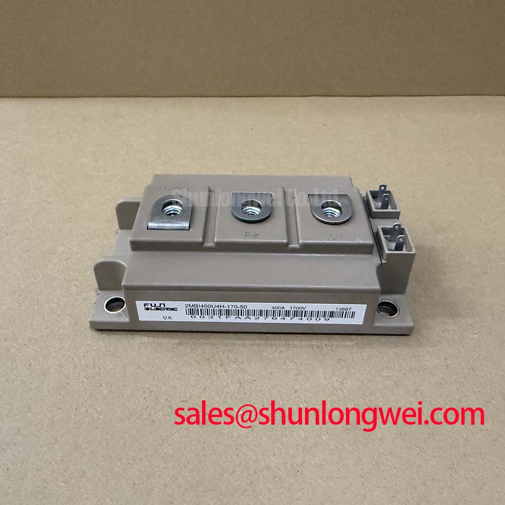
Operating high-power half-bridge modules like the 2MBI400U4H-170 in multi-megawatt wind turbine full-scale converters introduces severe electrical stress across both the power and signal planes. In a typical 690V AC converter setup, the intermediate DC-link bus routinely floats between 1050V and 1200V DC. At these voltage levels, incoming quality assurance (QA) protocols begin at the test bench with strict verification of package creepage distances and galvanic isolation barriers. The Fuji Electric 2MBI400U4H-170 is constructed in a robust dual-pack (half-bridge) topology rated for an absolute maximum collector-emitter voltage of VCES = 1700V (Official Datasheet Specification) and a continuous collector current of IC = 400A at TC = 80°C (Official Datasheet Specification). When screening incoming units prior to system integration, the external clearance over the package housing must measure at least 15 mm to satisfy reinforced isolation standards (such as IEC 61800-5-1) for industrial utility installations.
High-voltage switching events generate steep collector-emitter voltage gradients that can exceed 15 kV/µs during rapid turn-off. These steep transitions cause common-mode displacement currents to flow directly through the parasitic coupling capacitance of the gate driver isolation barrier. If the signal isolation transformer or digital optocoupler lacks adequate Common-Mode Transient Immunity (CMTI), transient currents can corrupt logic states and trigger catastrophic shoot-through events across the DC link. For reliable operation in offshore turbine converters, gate driver signal chains must feature a CMTI rating of at least 100 kV/µs (Design Consideration for 1700V Wind Inverter Topologies). PCB layout engineers must physically isolate primary control traces from secondary floating emitter references by milling isolation slots beneath optocouplers and maintaining a minimum of 8 mm clearance between high-voltage traces.
When bench-testing incoming modules, static verification of the gate-emitter leakage current and internal gate integrity is an essential preliminary diagnostic. A digital electrometer should be connected across terminals G1-E1 and G2-E2 to ensure that gate leakage remains strictly below 500 nA at an applied gate-emitter bias of VGE = ±20V. In complex power conversion assemblies, auxiliary circuits such as pre-charge controllers or active crowbar stages often interface with lower-current switches like the 2MBI200UD-120-51 to handle secondary system functions, making modular pinout and isolation verification across diverse module ratings standard practice during incoming hardware inspection.
| Parameter | Official Datasheet Value | Test / Operating Condition | Engineering QA Significance |
|---|---|---|---|
| Collector-Emitter Voltage (VCES) | 1700 V | Tj = 25°C, VGE = 0V | Provides breakdown headroom for 690V AC line wind converter DC links. |
| Continuous DC Current (IC) | 400 A | TC = 80°C, continuous | Determines continuous current carrying capacity of the power stack. |
| Saturation Voltage (VCE(sat)) | 2.30 V (typical) | IC = 400A, VGE = 15V, Tj = 125°C | Directly sets conduction loss dissipation during high-power operation. |
| Thermal Resistance (Rth(j-c)) | 0.045 °C/W | Per IGBT element, junction-to-case | Determines required heatsink thermal efficiency under full output. |
Negative Gate Bias vs Active Miller Clamping in Fast-Switching Half-Bridges
In bridge legs handling 400A continuous current, the parasitic Miller capacitance (collector-to-gate capacitance, Cres) represents a prominent vulnerability during high dv/dt switching transitions. When the lower IGBT turns off and the upper IGBT switches on, the rapid rise in the lower device's collector-emitter voltage injects displacement current directly into its gate node. If the gate drive output impedance is insufficient, this current charges the input capacitance (Cies) above the threshold voltage (typically VGE(th) between 5.5V and 7.5V for standard 1700V silicon dies), leading to cross-conduction shoot-through across the DC rail.
To secure noise immunity against parasitic turn-on, hardware designers implement either a robust negative gate off-state bias (typically -8V to -15V) or dedicated Active Miller Clamping (AMC). A steady negative bias increases the dynamic threshold margin, forcing any Miller displacement current to elevate the gate voltage only from a deeply negative baseline. When choosing an Active Miller Clamping circuit, the clamping transistor must be positioned as physically close to the module auxiliary gate-emitter terminals as possible, engaging a low-impedance path (Rclamp < 1.5 Ω) directly to the negative rail whenever the gate command drops below 2.0V.
When selecting driver components and studying high-voltage die structures across various industrial switching technologies, evaluating switching characteristics detailed in documents like Fuji Electric High-Speed Discrete IGBTs provides useful insight into dynamic charge distribution and internal capacitance behavior. For auxiliary supply design, floating DC-DC gate drivers must be sized to supply continuous current based on the total gate charge (Qg ≈ 3.8 µC at VGE = ±15V) and switching frequency (typically 2.5 kHz to 4.0 kHz in megawatt-scale wind converters), preventing bootstrap or isolated rail sag during continuous operation.
💡 Bench Tip: During incoming bench testing, always connect a 10 kΩ resistor between the gate and emitter auxiliary terminals before performing any diode forward drop or isolation continuity checks. An ungrounded gate picks up static electric charges that partially bias the channel, causing inaccurate multi-meter diode-check readings and exposing the internal gate oxide to destructive ESD stress.
DC-Link Capacitance Bank Layout and Low-ESL Busbar Interconnection Techniques
Turn-off transient voltages in 1700V modules are governed by the total parasitic stray inductance (Lσ) of the commutation loop. As the 400A collector current drops abruptly at rates exceeding 2000 A/µs during short-circuit turn-off or heavy-load commutation, the trapped magnetic energy induces a severe voltage spike that adds directly to the steady-state DC rail voltage. The instantaneous peak collector-emitter voltage reached during turn-off is defined by the sum of the DC-link voltage and the inductive voltage drop produced across the loop inductance during the current fall time (Vpeak = VDC + Lσ × di/dt). To keep peak voltage below the 1700V limit under 1150V DC operating conditions, the total loop inductance must not exceed 25 nH (Design Consideration for Low-Inductance Power Inverters).
Achieving this low inductance demands planar laminated busbar geometries where wide positive and negative copper conductor plates are interleaved with thin Mylar or Nomex dielectric insulation (0.5 mm to 1.0 mm thickness). Symmetrical plate overlapping forces opposing currents to flow through closely coupled paths, maximizing magnetic field cancellation. High-frequency polypropylene snubber film capacitors (0.47 µF to 1.0 µF, rated for 2000V DC) should be bolted directly across the DC terminals of the 2MBI400U4H-170 to suppress high-frequency ringing and clamp turn-off overshoots. For lower-voltage auxiliary systems operating from standard 400V/480V mains, designers often utilize lower-voltage modules such as the 2MBI400VB-060-50, which feature distinct busbar geometry and insulation spacing requirements.
⚠️ Field Alert: When mounting the module to the DC-link busbars, strictly observe terminal screw thread depths and torque limits. Applying over-torque to the M6 power terminals (recommended torque: 3.5 to 4.5 N·m) can crack the internal terminal bonding substrates, while under-torque creates loose contact interfaces with localized heating, causing thermal runaway under sustained 400A RMS operation.
Thermal Feedback & V_CE(sat) Positive Temperature Coefficient Equalization
In high-power wind turbine converters, multiple half-bridge modules are regularly operated in parallel to achieve megawatt-level inverter outputs. A critical operational attribute of the 2MBI400U4H-170 is the positive temperature coefficient of its saturation voltage, VCE(sat). While standard silicon displays a slightly negative temperature coefficient at low current densities, the module transitions to a strong positive temperature coefficient above 150A, exhibiting a typical saturation voltage of 2.30V at Tj = 125°C compared to 1.95V at Tj = 25°C. When two or more modules share current, any module carrying disproportionate load heats up, naturally elevating its internal dynamic resistance and diverting subsequent current to cooler parallel branches, providing inherent protection against thermal runaway.
While steady-state static current sharing is self-equalizing via the positive VCE(sat) coefficient, dynamic current balancing during rapid turn-on and turn-off transients depends entirely on circuit symmetry. Unbalanced stray inductance between parallel branches or mismatched gate drive trace lengths will force one module to handle peak transient currents during switching intervals. To achieve dynamic current balance within 5% deviation across parallel power legs, engineers must apply symmetrical star-point gate wiring layouts, match external gate resistor values (RG(on) and RG(off)) to within 1% tolerance, and utilize twisted-pair cabling for all auxiliary emitter feedback connections.
Effective thermal dissipation from the module baseplate to the liquid-cooled cold plate relies on precise interface preparation. The junction-to-case thermal resistance is rated at Rth(j-c) = 0.045 °C/W (Official Datasheet Specification). To maintain low junction temperatures under variable wind gusts, thermal interface material (TIM) must be applied with a screen-printed pattern to achieve a uniform wet thickness between 80 µm and 100 µm. Cold-plate surface flatness must not deviate by more than 50 µm over a 100 mm span. Tightening the M5 baseplate mounting bolts in a crosswise progressive pattern (0.5 N·m initial torque, followed by final torque of 2.5 to 3.5 N·m) prevents baseplate deformation and ensures uniform void-free contact across the entire copper thermal footprint.
Standardized incoming inspection procedures, thermal resistance verifications, and degradation monitoring strategies are outlined in detail within the Field Engineer’s Handbook, which serves as a technical resource for evaluating semiconductor reliability in utility-scale renewable energy installations.