Content last revised on September 27, 2026
Field Diagnostics and Commissioning for Dynamic Power Loss in 2MBI450VJ 120 50 Topologies
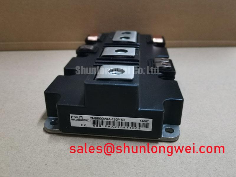
Begin commissioning by isolating and discharging the DC link, confirming the module marking against the approved bill of materials, and inspecting the housing, terminals, mounting surface, and insulation barriers before any energized test. The 2MBI450VJ 120 50 is a Fuji Electric 2 in 1 half bridge IGBT module with an official collector emitter voltage rating of 1200 V and a continuous collector current rating of 450 A under the specified datasheet conditions. These are device ratings, not automatic permission to operate a complete traction inverter at those limits. The switching frequency, cooling system, duty cycle, overload profile, bus voltage, gate driver behavior, and commutation conditions must be verified at system level.
The collector emitter saturation voltage must be evaluated using the applicable datasheet values and their stated collector current, gate voltage, and junction temperature conditions. During a controlled low energy test, compare the measured saturation behavior of the installed module with the approved reference data and the known good phase leg. A higher reading can increase conduction dissipation, while a lower or unstable reading should be assessed together with gate voltage, collector current, junction temperature estimation, probe placement, and switching state. A single voltage reading is not sufficient to establish module health.
| Official parameter | Published value | Engineering significance |
|---|---|---|
| Collector emitter voltage | 1200 V | Defines the stated blocking voltage capability of the IGBT structure |
| Continuous collector current | 450 A under the specified datasheet conditions | Provides the stated continuous current reference for thermal and electrical evaluation |
| Collector emitter saturation voltage | Refer to the applicable datasheet values and test conditions | Directly affects conduction loss and cooling requirements |
| Module configuration | 2 in 1 half bridge | Integrates the upper and lower switching positions in one power module |
For pulsed overload analysis, use the junction to case thermal impedance information from the applicable Fuji Electric documentation and, where provided, represent the transient response with the documented multi RC network. The thermal estimate should follow the actual pulse width, repetition pattern, case temperature, switching loss, conduction loss, and cooling boundary. A peak junction temperature calculation is an engineering calculation only when the thermal model, loss waveform, and measurement assumptions are recorded. The result should then be checked against the manufacturer specified operating limits.
When a locomotive traction inverter or high speed rail converter is being assessed, inspect phase current balance, gate timing, heat sink temperature distribution, and the DC link waveform under controlled acceleration and regenerative conditions. The device should be evaluated as one part of the commutation loop. The inverter designer remains responsible for confirming creepage, clearance, insulation coordination, current sensor bandwidth, protection response, and the relationship between peak switching voltage and the 1200 V device rating.
Thermal Interface Control and Protection Reliability
The baseplate interface has a direct effect on the thermal path from the module to the heat sink. A design consideration for this class of power assembly is to apply a controlled, uniform thermal interface layer, remove trapped air, and verify that the heat sink surface is clean and suitably flat. The frequently used 50 to 100 micrometre interface range is a general assembly reference, not an official published parameter of this module. The system manufacturer should confirm the approved compound, application method, surface tolerance, and production inspection method.
Mounting screws should be tightened in a staged and diagonal sequence so that the baseplate is seated progressively rather than pulled down at one corner. The applicable Fuji Electric mechanical specification must take priority for screw type, washer arrangement, torque, and tightening order. Where the heat sink or baseplate shows curvature, do not compensate by excessive fastener force. Recheck the mechanical stack, contact pattern, surface condition, and interface material distribution before accepting the assembly.
Protection coordination should combine desaturation or overcurrent detection, gate driver fault handling, DC link monitoring, and a semiconductor fuse selected from the converter fault study. The fuse clearing time and let-through I2t must be evaluated against the relevant circuit withstand limits; I2t alone does not establish IGBT short circuit protection. The driver detection and turn off sequence must separately be checked against the documented short circuit withstand conditions. A fuse rating based only on the 450 A continuous current value does not establish protection during a dead short. The interruption time, prospective fault current, stray inductance, driver delay, and fault energy all require validation.
Do not transfer thyristor gate parameters such as IGT and VGT to this IGBT module. Those values describe thyristor triggering and are not substitutes for the IGBT gate voltage, gate resistance, gate charge, short circuit withstand, or driver timing data required by the applicable Fuji Electric data sheet. If a converter includes thyristor stages elsewhere in the power path, its pulse train and trigger margin should be assessed separately.
For a high side gate supply using a bootstrap arrangement, capacitor selection is an engineering calculation based on gate charge, driver quiescent current, leakage, switching duration, refresh interval, temperature, and allowable gate supply ripple. The correct value cannot be derived from the module current rating alone. Designers should verify that the bootstrap supply remains within the driver operating window during the longest high side conduction interval and during repeated regenerative transitions. An isolated gate supply may be evaluated when the topology or duty cycle does not provide adequate refresh conditions.
Safety reminder: isolate and discharge the DC link before connecting, removing, or probing any gate or power terminal.
Parallel Module Current Sharing and Gate Loop Verification
Parallel operation requires more than connecting equal length power cables. The module data, current waveform, gate driver capability, thermal path, and protection response must support the intended arrangement. The positive temperature coefficient associated with IGBT saturation voltage can assist static current sharing as temperature changes, but it does not guarantee balanced dynamic current during turn on, turn off, short circuit interruption, or diode commutation.
Use symmetrical collector and emitter bus geometry, matched gate loop routing, and a common reference strategy appropriate to the driver design. The gate path should be treated as a high di/dt switching loop. Minimize parasitic inductance to reduce unwanted gate voltage movement and Miller coupling, then verify the result with differential probes at the module terminals. The acceptable overshoot and ringing limits must be established by the system engineer against the gate driver and device documentation.
During commissioning, compare the current waveform of each parallel branch using calibrated sensors with consistent bandwidth and probe placement. Check turn on delay, turn off delay, collector emitter voltage transition, gate voltage plateau behavior, and temperature rise over the intended load range. A branch that appears balanced at low current may diverge at higher current because of driver impedance, busbar asymmetry, thermal differences, or unequal commutation paths.
When the module is considered for a replacement evaluation, the electrical topology and mechanical interface must be compared directly with the original assembly. The 2MBI400U4H 170 can be reviewed as a separate reference device, but its voltage class, current capability, package details, switching data, and gate requirements must not be assumed interchangeable with the 2MBI450VJ 120 50.
Use an oscilloscope to investigate abnormal ringing or unequal current rather than assigning a single cause from a visual symptom. Verify the measurement loop, sensor polarity, driver reference, gate resistor population, emitter return path, and dead time. Where a fault appears only during regenerative operation, include the freewheel diode recovery waveform and commutation layout in the investigation. The diode softness factor S, reverse recovery charge, and reverse recovery current, where documented, must be taken from the relevant device documentation; they should not be inferred from the IGBT part number.
DC Link Capacitor Bank Layout and Low Inductance Switching Tests
Inspect the DC link capacitor bank, laminated busbar, module terminals, snubber connections, and return path as one commutation structure. The design objective is to minimize the parasitic loop inductance that converts switching current slew into collector emitter overshoot. In practical testing, the peak voltage can be interpreted through the relationship between the DC link voltage, loop inductance, and current change rate, but the resulting limit must be confirmed with a properly compensated high voltage probe at the module terminals.
A short, wide, and symmetrical busbar arrangement usually provides a more predictable current path than long point to point wiring. Place the high frequency capacitor connection close to the switching loop, keep forward and return conductors adjacent where the insulation system permits, and avoid routing sensitive gate or feedback wiring beside the highest current edge. Any target such as a 25 nH loop value is a system design objective requiring extraction or measurement; it is not an official 2MBI450VJ 120 50 specification.
Snubber selection should begin with the measured voltage waveform, switching energy, ringing frequency, capacitor dielectric behavior, resistor pulse capability, and thermal loss. Increasing capacitance can reduce an edge amplitude in some circuits while increasing switching loss in others. Designers should test the selected network at the intended DC link voltage, load current, temperature, and switching speed, then verify that the IGBT and diode losses remain acceptable.
For field troubleshooting, first confirm that the oscilloscope probe has adequate voltage rating and a low area connection. Then compare the DC link waveform at the capacitor bank with the waveform at the module terminals. A large difference may indicate busbar inductance, connection geometry, probe error, or a commutation path that is not represented in the schematic. Check capacitor ESR, terminal integrity, laminated conductor alignment, and snubber connections before changing gate resistance.
The external packaging literature on flip chip packaging with copper pillar bumps for low parasitic inductance provides useful background on interconnect inductance, but it does not define the internal construction or performance of this Fuji Electric module. For a broader comparison of 1200 V switching technologies in three phase conversion, engineers may also consult The 1200 V CoolSiC MOSFET Advantage in Three Phase Power Conversion. Such references support topology evaluation; they do not replace the Fuji Electric data sheet or the measured switching validation for the 2MBI450VJ 120 50.
For high speed rail and heavy freight locomotive traction inverter evaluations, the final acceptance record should include the verified module identity, electrical ratings, gate driver waveforms, thermal measurements, current sharing results, DC link overshoot, protection timing, and mechanical installation records. The system integrator should confirm compatibility with the original traction converter documentation before any replacement or production release.