Content last revised on September 9, 2026
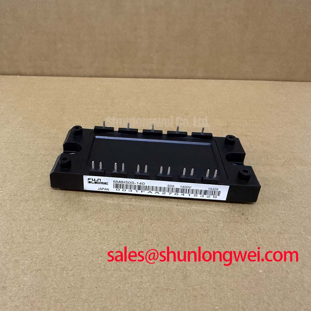
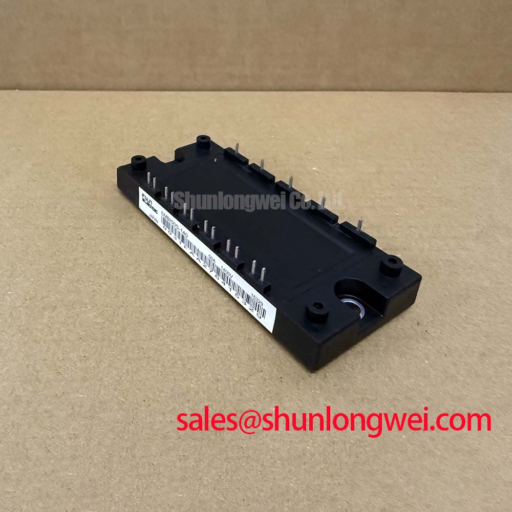
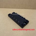
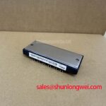
Fuji Electric 6MBI50S-140 Overview
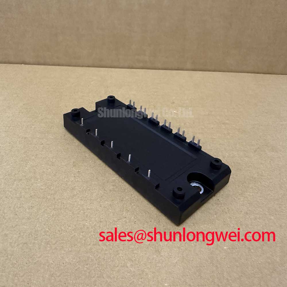
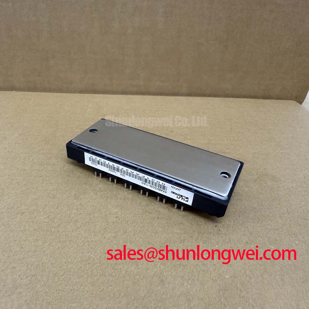
Before energizing a replacement, isolate the DC link, inspect the module body and terminals, and verify the nameplate boundary of 1,400 V and 50 A against the equipment service record. The Fuji Electric 6MBI50S-140 is an IGBT Module in a module package. These three official product parameters define the basic identity supplied for this product page: specified voltage rating 1,400 V, rated current 50.0 A, and package type Module.
For an industrial inverter welder or medium frequency induction heating power supply, those values should be treated as component ratings rather than as a complete system operating envelope. The actual usable current depends on switching frequency, conduction duty, cooling conditions, junction temperature, gate drive behavior, commutation layout, and the protection strategy implemented by the equipment manufacturer. The system integrator should confirm every additional electrical and thermal limit from the original Fuji Electric documentation and the equipment service manual.
| Manufacturer | Fuji Electric |
| Part number | 6MBI50S-140 |
| Product category | IGBT Module |
| Specified voltage rating | 1,400 V, Official Specification |
| Rated current | 50.0 A, Official Specification |
| Package | Module, Official Specification |
Field Diagnostics & Commissioning: Transmission Line Impedance Mismatch in 6MBI50S-140 Topologies
Begin commissioning with the power stage disconnected from the load where the equipment procedure permits it. Check the DC bus polarity, the gate driver supply, the emitter reference, and the continuity of the control interlock. A cold resistance test between power terminals can help identify an obvious shorted semiconductor, but it is only a screening method. Semiconductor junction readings vary with the test instrument, connected snubbers, parallel paths, and the circuit topology. A result that appears unusual should be compared with a known-good phase and then verified using an isolated oscilloscope measurement.
Long motor leads and loosely arranged bus conductors can behave like a transmission path rather than an ideal wire. During turn-off, stray inductance interacts with the switching current and can create a terminal overshoot that is substantially higher than the measured steady DC-link voltage. The often-cited possibility of a spike approaching twice the bus voltage is a system-level warning, not an official rating or a guaranteed behavior of this module. Engineers should capture collector to emitter voltage directly at the module terminals while observing gate voltage, phase current, and DC-link voltage on the same switching event.
When a field waveform shows ringing, first separate the possible sources. Compare the waveform at the module terminals with the waveform at the inverter output and at the load-side cable entry. A large difference between these locations may indicate impedance mismatch, probe-loop pickup, cable resonance, or a commutation path with excessive parasitic inductance. Use a properly rated differential probe, keep the measurement loop compact, and repeat the test at representative load current. Do not use a long ground lead on a conventional oscilloscope probe for a high-current switching node.
Output filters and chokes should be selected from the complete motor or heating-load network, not from the module current number alone. The designer should consider cable length, switching frequency, common-mode behavior, winding insulation stress, thermal dissipation, and the filter’s effect on control-loop stability. A filter that reduces ringing can also increase stored energy and alter the turn-off current path. Its final value and damping arrangement require system simulation followed by double-pulse or controlled load testing.
Clearance and creepage around the power terminals should follow the applicable equipment insulation rules and the contamination level of the enclosure. Keep gate wiring away from the collector and switching output conductors, and route the return path with the signal path rather than treating the chassis as an assumed high-frequency reference. 💡 Pro Tip: Disconnect the DC link and wait for the equipment discharge verification before removing the module or attaching oscilloscope accessories.
Transient Dynamics & Electrical Design: Overvoltage Trip Prevention During Fast Switching
In regenerative inverter systems, motor deceleration can return energy to the DC link faster than the line-side converter can remove it. A braking chopper path then transfers selected energy into a high-power ballast resistor. The 6MBI50S-140 may be evaluated in such a topology only after the engineer confirms the complete chopper duty, pulse energy, resistor thermal behavior, DC-link control threshold, and semiconductor switching stress. The module’s official 1,400 V rating should not be interpreted as permission to operate continuously at that voltage under every switching and thermal condition.
The braking resistor must be assessed for both instantaneous pulse absorption and repetitive average dissipation. A resistor that survives a single deceleration event may still overheat during repeated cycles. Review the machine’s stop profile, inertia, maximum speed, deceleration command, regeneration interval, and cooling airflow. The overvoltage trip setting should coordinate with the semiconductor voltage boundary, measurement tolerance, turn-off overshoot, and the response delay of the control system. Final values are system-determined and must be validated under the highest credible regenerative condition.
Fast switching makes the gate-drive loop part of the power circuit. The driver should provide a controlled turn-on and turn-off path, a defined emitter reference, and protection against unintended gate charging caused by the Miller effect. Dead-time must prevent complementary devices from conducting simultaneously, while excessive dead-time can increase diode conduction and commutation loss. Engineers should verify the timing at the actual module terminals, including propagation delay, driver saturation, temperature variation, and the behavior of the fault shutdown path.
For a high-side driver using a bootstrap supply, capacitor selection is governed by the gate charge demanded during the intended pulse sequence, driver quiescent current, leakage, bootstrap diode behavior, switching frequency, and the allowable supply droop. The correct capacitance is therefore a calculated system value based on the selected gate driver and the confirmed module gate-charge data. Since that gate-charge information is not included in the supplied product parameters, it should not be inferred here. The system designer should obtain it from the applicable Fuji Electric datasheet before sizing the bootstrap network.
During commissioning, observe the gate to emitter voltage at the module rather than only at the driver output. A clean driver waveform at the control board does not prove that the same waveform reaches the power terminals. Check for negative excursions, excessive ringing, delayed turn-off, and differences between parallel gate paths. A gate resistor, ferrite element, or Miller clamp can be considered when the measured waveform shows susceptibility to false turn-on, but the choice should be made from measured switching loss and transient behavior rather than a universal preset value.
Fuji Electric’s information on brake chopper IGBT modules provides useful manufacturer context for regenerative braking topologies. It should be read alongside the specific documentation applicable to the installed module and the inverter’s protection circuit.
6MBI50S-140 Operational Boundaries: Evaluating Cosmic Ray Robustness and Voltage Derating
Cosmic-ray and terrestrial-neutron effects are reliability topics that cannot be converted into a credible failure-in-time figure from the supplied product data. No authoritative SEB test result, neutron cross-section, FIT value, altitude derating curve, or cosmic-ray qualification statement has been provided for this product page. It would therefore be technically improper to claim a specific burnout probability or to calculate a guaranteed failure rate above a particular elevation.
Altitude can influence cooling performance, insulation coordination, and the environmental conditions surrounding the inverter. At higher elevations, reduced air density may affect heat transfer and external insulation margins, but the appropriate correction depends on the enclosure, cooling method, pollution level, spacing, operating voltage, and applicable equipment standard. Designers should obtain the manufacturer’s environmental and insulation guidance before approving operation at elevated sites.
For practical validation, record the maximum DC-link voltage, switching overshoot, operating temperature, and load current during the most demanding operating sequence. Compare the measured peak collector to emitter stress with the official device limits from the relevant datasheet, allowing the equipment designer to establish a documented derating policy. The voltage headroom should account for measurement uncertainty, control tolerance, transient repetition, and changes caused by cable routing or filter configuration.
If a field unit fails during a high-energy switching event, avoid assigning the cause to cosmic radiation from the symptom alone. Inspect the gate waveform, busbar joints, snubber condition, overvoltage trip history, cooling path, and the timing of the protection circuit. Compare the failed phase with the corresponding healthy phase and preserve the event records where available. This approach can distinguish a switching transient, gate-drive fault, thermal overload, or assembly issue from an unverified single-event mechanism.
Designers evaluating newer wide-bandgap alternatives should keep the comparison neutral and system-based. Switching speed, gate-drive requirements, insulation stress, EMI behavior, short-circuit response, and thermal design can differ materially between silicon IGBT modules and SiC or GaN solutions. The engineering background article Wide Bandgap Revolution can support that broader technology comparison without being treated as a specification for this Fuji Electric module.
6MBI50S-140 Operational Boundaries: Evaluating Thermal Feedback Limits
Parallel IGBT operation requires attention to both static current sharing and dynamic switching balance. The positive temperature coefficient commonly associated with on-state collector-emitter saturation behavior can support static sharing because a warmer device tends to develop a higher conduction voltage. This is a design consideration, not a guarantee that arbitrary parallel wiring will share current safely. Differences in thermal contact, gate threshold, stray inductance, driver delay, and emitter path resistance can still force one device to switch or conduct more heavily.
When multiple modules are considered for a higher-current stage, use symmetrical busbar geometry and matched electrical path lengths. The gate drive should have a controlled reference for each device, with the power emitter and gate-return arrangement designed to prevent one device’s switching current from modulating another device’s gate signal. The exact wiring method depends on the module terminal arrangement and the driver architecture, so the original mechanical drawing and application documentation must be checked before fabrication.
Thermal validation should measure the temperature of each parallel position under steady load and during the most demanding switching sequence. A shared heatsink does not automatically produce equal junction conditions. Verify mounting flatness, interface consistency, airflow distribution, and the temperature response after repeated load cycles. The allowable operating point must be established from the official electrical and thermal specifications, the heatsink capability, and the measured case-to-junction behavior of the complete assembly.
Dynamic imbalance is often revealed by unequal collector current rise, different turn-off tails, or inconsistent voltage overshoot between parallel branches. Use isolated current measurement and carefully synchronized voltage probes to compare devices under the same command pulse. If the waveforms diverge, inspect gate-loop inductance, resistor tolerance, driver output impedance, busbar symmetry, and local decoupling before changing the control timing. A microsecond-scale buffer or additional dead-time may be considered only after the measured commutation event shows that it is necessary and that the resulting conduction loss remains acceptable.
For system-level reference, engineers can review Fuji Electric’s 7th-Generation X-Series IGBT module information when comparing technology platforms, switching characteristics, and application documentation. For a neutral cross-reference exercise within the same supplier catalog, the 6MBI15L-060 can be reviewed as a separate product rather than assumed to be a direct replacement. In a related power topology, the 6MBI100L-060 may be evaluated as a separate front-end or complementary-stage device, subject to voltage, current, thermal, and control compatibility checks.
Before releasing the repaired inverter welder or medium-frequency induction heating supply, repeat insulation checks, gate-drive checks, low-energy switching tests, controlled load tests, and protection-trip verification. The 6MBI50S-140 identity supplied here remains 1,400 V, 50.0 A, and Module package; every system-specific limit must be confirmed against the applicable Fuji Electric documentation and measured in the finished equipment.