Content last revised on September 10, 2026
6MBP100NA060-01 Fuji Electric 600V 100A IPM Module with 6-Pack IGBT and Brake Chopper
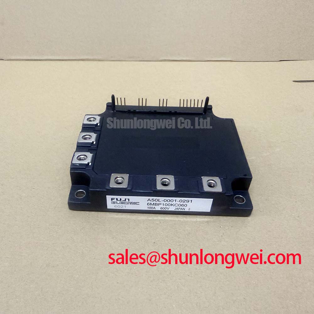
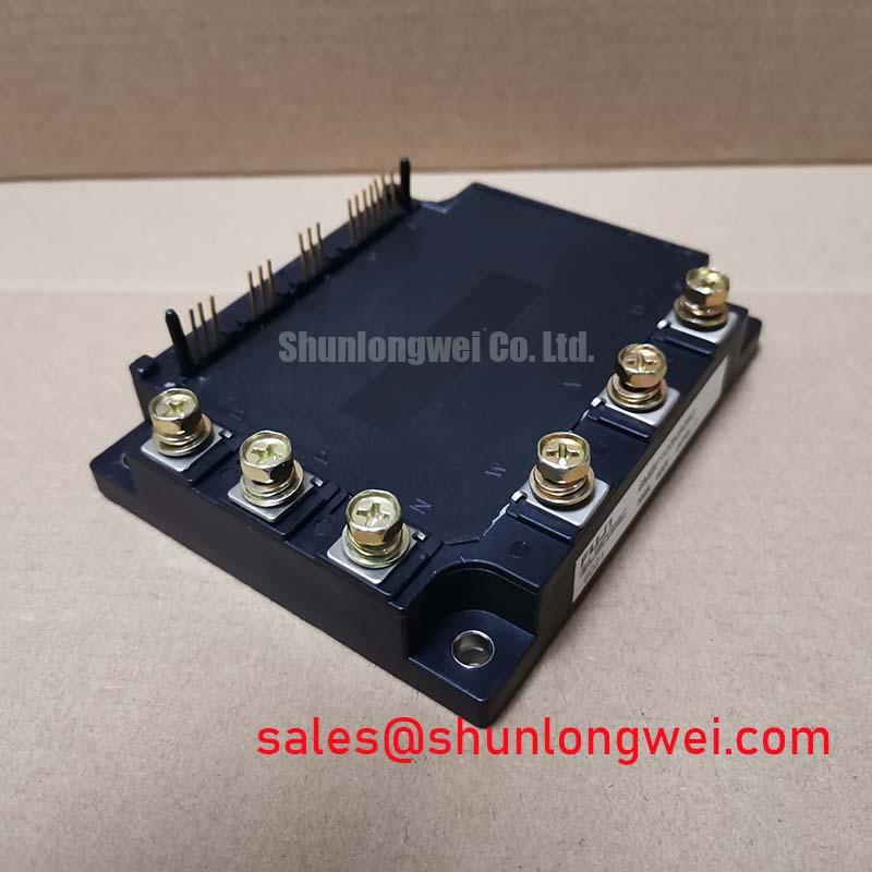
With the DC link fully discharged, begin a replacement check by recording the module marking, inspecting the power terminals and baseplate for mechanical damage, and comparing cold-state terminal impedance with a known-good unit from the same drive. The 6MBP100NA060-01 is a Fuji Electric IPM module specified for a 600 V collector-emitter voltage and 100 A collector current, with an integrated six-IGBT power stage, brake chopper, and NTC thermistor.
| Parameter | Official Specification | Engineering Interpretation |
|---|---|---|
| Manufacturer | Fuji Electric | Confirm the original drive documentation and terminal layout before installation. |
| Product category | IPM Module | Combines a three-phase IGBT power section, brake chopper, and temperature-sensing NTC in one power module. |
| Collector-emitter voltage, VCES | 600 V | Defines the module’s voltage class; suitability for a particular AC supply depends on the complete DC-link, transient, and protection design. |
| Collector current, IC | 100 A | Use the stated current rating only with the applicable thermal, switching, overload, and duty-cycle conditions verified at the system level. |
| Collector-emitter saturation voltage, VCE(sat) | 2.2 V typical, 2.7 V maximum | Use the maximum value when estimating conduction loss unless the system calculation defines another applicable condition. |
| Integrated topology | IGBT 6-pack + brake chopper + NTC thermistor | Reduces the number of separate high-power switching assemblies in a compatible VFD design. |
| Overheat protection temperature, Tj | 150 °C | Treat this as a protection-related temperature specification rather than a normal operating target. Confirm how the drive uses the NTC and any module protection signal. |
Assembly Integrity & Layout Architecture: Implementing Thermal Feedback for 6MBP100NA060-01
Before removing a failed module, photograph the original busbar, gate-driver, NTC, and auxiliary connections. This prevents a wiring error from being mistaken for a defective replacement. The power terminals should be checked for discoloration, looseness, cracked solder joints, and evidence of uneven clamping. The baseplate and heatsink contact area also deserve inspection because a flat electrical replacement can still fail thermally if the mounting surface is contaminated or distorted.
The six-IGBT topology requires symmetrical current paths wherever the mechanical layout permits. Keep the phase-leg power conductors short and physically grouped, while routing gate-driver conductors away from high-current commutation paths. Gate-loop inductance can produce ringing, false turn-on, and uneven switching between parallel paths. This is a Design Consideration, not a Fuji Electric guaranteed installation value. The final arrangement should be checked with an oscilloscope during controlled switching tests, using suitable differential and isolated current probes.
The integrated NTC thermistor can provide a temperature-feedback signal to the drive controller when it is correctly connected to the applicable sensing circuit. Its resistance should be evaluated against the original system documentation rather than assigned a generic pass or fail threshold. A cold resistance measurement can identify an open circuit, a shorted sensing path, or wiring continuity problems, but it does not prove the thermal interface is correct. During commissioning, compare the NTC trend with heatsink temperature and load current so that the controller is responding to a credible thermal signal.
VCE(sat) generally increases with junction temperature, which can support static current sharing when devices operate under suitably matched conditions. Dynamic sharing is more sensitive to gate resistance, driver propagation delay, stray inductance, and busbar symmetry. Designers should therefore match the physical gate paths and verify turn-on and turn-off waveforms at the actual operating voltage. The 6MBI100L-060 may be evaluated as a separate, objectively specified product when the original equipment documentation permits comparison; electrical ratings, pin arrangement, thermal interface, and protection behavior must be checked independently.
⚠️ Field Alert: Isolate the DC link and follow the equipment discharge procedure before touching power, gate, or NTC connections, even when the drive display is blank.
6MBP100NA060-01 Operational Boundaries: Evaluating Thermal Time Constants and Peak Junction Limits
The stated 150 °C Tj overheat protection temperature is an important system boundary, but it is not a complete thermal design prescription. A drive engineer must combine the module’s official thermal data, heatsink characteristics, ambient conditions, switching frequency, motor current waveform, overload duration, and enclosure airflow. If the detailed thermal resistance or transient impedance data is not available for the intended operating point, the peak junction temperature cannot be established reliably from the 100 A label alone.
For a pulsed overload, evaluate the thermal response as a transient network rather than relying only on steady-state heatsink temperature. A multi-RC model can represent the junction-to-case response, while the measured case temperature provides the boundary condition for the calculation. The calculation should use the applicable switching and conduction losses, with VCE(sat) treated according to its specified typical and maximum values. The result must be verified against the manufacturer’s permitted operating conditions and the drive’s actual overload profile.
Busbar geometry is a practical source of switching overshoot. Minimize the commutation loop area and place the DC-link film capacitor close to the switching power path when the system architecture allows it. Snubber selection and placement should be based on measured ringing, peak voltage, pulse energy, and capacitor temperature rather than on a generic capacitor value. The system designer must verify peak collector-emitter voltage during the fastest intended switching event and compare it with the 600 V VCES official specification.
During a field inspection, look for a thermal pattern that changes with load direction, carrier frequency, or braking activity. A phase terminal with a different temperature trend may indicate unequal contact pressure, busbar asymmetry, gate-drive mismatch, or a motor-side fault. These observations are diagnostic clues rather than single-cause proof. Confirm them by measuring phase current balance, gate-emitter waveforms, DC-link ripple, and the NTC signal under a controlled low-energy test.
6MBP100NA060-01 Circuit Diagnostics & Commissioning: Verifying Gate-Drive Architecture
The 6MBP100NA060-01 specification supplied here identifies the power topology and NTC function, but it does not establish an integrated active Miller clamp, a negative gate-bias requirement, or a particular gate-driver circuit. If the existing VFD uses an active Miller clamp, isolated gate feedback, bootstrap charging, or negative turn-off bias, the replacement must be assessed against the original driver architecture. The system integrator should verify the required gate voltage, isolation arrangement, dead time, and supply sequencing from the drive schematic and the applicable Fuji Electric documentation.
High dv/dt can couple through the gate-collector capacitance and raise the inactive device gate voltage. A Design Consideration is to use a low-impedance turn-off path and, where supported by the driver, an active Miller clamp positioned close to the relevant gate-emitter loop. The clamp should engage only after the gate command has reached its intended off state, with timing coordinated to avoid interference with the complementary switch. Oscilloscope verification should include both the commanded gate signal and the actual gate-emitter voltage at the module terminals.
Do not infer a damaged IGBT from a single resistance reading. First isolate the driver supply and ensure the DC link is discharged, then test the power terminals and gate paths with the module disconnected from the controller. Compare all equivalent phase positions, inspect for gate resistor cracking, and check whether the NTC circuit is being interpreted correctly. Abnormal readings may originate in the driver board, an attached snubber, motor cable insulation, or a shorted load. A controlled current-limited energization is more informative than immediately applying full DC-link voltage.
If the drive uses a bootstrap arrangement, the high-side driver supply must recharge under the actual low-side conduction and duty-cycle conditions, while diode recovery and local loop inductance can affect gate voltage stability. The required capacitor, diode, and switching timing are system-determined; they should be verified from the original gate-driver design rather than guessed from the module current rating. For motor-control theory, the Clarke Transformation reference is useful when checking phase-current interpretation, while BLDC commutation provides relevant background for electronically switched motor systems.
6MBP100NA060-01 Circuit Protection & Reliability: Calibrating Dynamic Braking Chopper Operation
The integrated brake chopper allows a compatible drive to manage DC-link energy during motor deceleration, but the module alone does not determine the braking resistor rating, duty cycle, or allowable regeneration profile. The resistor must be selected from the motor and load inertia, commanded deceleration, DC-link behavior, braking repetition, enclosure temperature, and the drive manufacturer’s protection settings. The chopper’s switching waveform and resistor temperature should be verified under the most demanding permitted braking sequence.
When a drive trips during deceleration, inspect the DC-link voltage trend, brake-command signal, chopper gate waveform, resistor wiring, and cooling path together. A trip may involve excessive regenerated energy, incorrect threshold calibration, an open resistor, a failed gate driver, poor busbar connection, or a motor-control setting that demands more braking than the mechanical system can dissipate. Avoid treating the brake chopper as a substitute for a properly coordinated overvoltage protection strategy.
The NTC should be included in the protection sequence where the controller supports it. A rising temperature signal can be used as a condition for alarm, controlled reduction of load, or shutdown, subject to the equipment safety design. The stated 150 °C Tj overheat protection temperature should not be repurposed as a normal operating target. Thermal alarms, overcurrent protection, short-circuit response, and DC-link overvoltage protection need coordinated testing at the complete drive level.
For applications involving motor braking or unusual regeneration behavior, consult the applicable drive, braking-resistor, and equipment documentation rather than inferring performance from unrelated converter topologies. The 6MBP100NA060-01 should be released for service only after terminal mapping, gate-drive compatibility, NTC feedback, thermal contact, current sharing, switching overshoot, and braking response have all been checked against the original equipment design.