Content last revised on October 20, 2026
Benchtop Waveform Tuning: Mechanical Stress Control for 6MBP100VDA060-50
With the drive isolated and its DC link confirmed discharged, inspect the module terminals for looseness, discoloration, or movement before reconnecting the power stage. 6MBP100VDA060-50 is a Fuji Electric IPM Module with a stated rated voltage of 600 V and rated current of 100 A, in a Fuji Power Module package. These ratings do not, by themselves, establish permissible operating conditions for a particular drive.
For a heavy-duty variable-frequency AC motor drive, confirm the exact part marking and compare the module’s pin layout and mounting interface with the unit being serviced before fitting it. Treat switching limits, protection behavior, and driver requirements as system-level compatibility checks. A mismatch in control interface or mechanical fit can prevent commissioning even when the headline voltage and current ratings appear suitable.
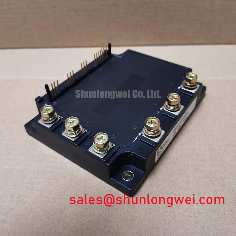
Check terminal engagement and clamping before using switching waveforms to diagnose a drive fault. A power-terminal connection that bottoms out, sits at an angle, or bears unevenly on its washer can transfer assembly force into the busbar interface. Vibration and repeated thermal cycling can aggravate that mechanical loading, so inspect the contact surfaces and fastener seating when a unit has been removed from a cabinet.
As a Design Consideration, use fasteners that match the equipment’s specified thread, length, and hardware stack. Confirm that the screw engages securely without bottoming in the terminal, and that the washer bears flat rather than bridging an edge or tilted surface. The module should sit flush on its mounting plane; do not use the power terminals to pull a misaligned assembly into position. Check cable and busbar routing for side load, and leave enough clearance to prevent conductors from pressing against the housing during installation.
When a vibration-related interruption is reported, compare the installed hardware with the drive’s assembly drawing, then inspect for movement, witness marks, or uneven contact pressure. These observations help distinguish a mechanical connection issue from a switching fault. If waveform tuning follows, capture signals using the intended probe connection and operating conditions; do not attribute ringing to the module until the measurement setup and busbar geometry have also been assessed.
Field Alert: Tighten terminals and mounting hardware to the equipment manufacturer’s specified procedure, and do not compensate for a poor fit by applying extra torque.
Field Diagnostics & Commissioning: Driver Power Sequencing
Establish stable auxiliary supplies for the IPM’s integrated gate-drive circuitry and verify the system’s inhibit and undervoltage-lockout behavior before enabling the high-voltage DC link. Confirm control-supply voltages, input signal levels, and sequencing against the module’s applicable manufacturer data and the drive documentation. Do not apply an external negative gate-bias supply to the IPM’s logic inputs.
During commissioning, first check that each control channel starts in its intended safe state and that a missing or unstable auxiliary rail keeps switching disabled. Verify the interlock response using the drive’s approved commissioning procedure. Only proceed to DC-link energization after the control supply, fault handling, and inhibit path behave consistently. This sequence limits the chance that a transient supply condition is mistaken for a module failure.
The IPM incorporates gate-drive circuitry; external gate-resistor tuning should not be assumed available. As a Design Consideration, assess control-input and supply waveforms at the documented module terminals with suitable isolated measurement equipment. Look for excessive ringing, slow input transitions, or unintended excursions, and review probe placement before changing interface components. Adjustments should be validated across the relevant operating states rather than inferred from a single unloaded bench test.
In a drive with isolated control channels, check the control-interface isolation and signal path as part of the same commissioning review. Common-mode transients can disturb control signals when the isolation interface, layout, or measurement arrangement is unsuitable. The Delta-Sigma Modulation (ADC) in Isolated Phase Current Sensing ICs reference describes a general conversion method; it is not a specification for this IPM or its gate driver.
Operational Boundaries: Power and Control Return Paths
Identify the power terminals and control connections from the module’s correct pinout before tracing the control-supply returns. Do not assume that a main load-current terminal and a control reference connection are interchangeable. Confirm each reference terminal’s function and location from the manufacturer’s pin diagram for the exact device revision; do not assume that an accessible auxiliary emitter or Kelvin gate-drive return is provided.
Route each control signal close to its specified reference path to reduce coupling from the high-current commutation path. Keep that control loop away from switching nodes where practical, and avoid sharing a narrow return path with noisy power current. These are general Design Considerations, not guarantees of a particular module layout. The system designer should check clearances, insulation coordination, and mechanical routing against the actual assembly.
If the drive shows intermittent triggering or inconsistent switching, compare control-input measurements at the module with the controller output and inspect the reference path for unintended shared impedance. A waveform that changes with probe grounding can reflect the measurement setup rather than the circuit itself. Use appropriately rated differential or isolated probes and verify the signal path against the drive schematic before changing the layout.
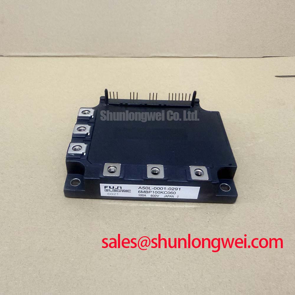
For an alternative within the same broad product family, the 6MBP100KC060 can be reviewed as a separate candidate. Do not treat the shared family naming as proof of pin, protection, or electrical interchangeability; compare the complete datasheets and the equipment interface before considering substitution.
Transient Dynamics & Cold Bench Screening
Before applying power, disconnect the module from the discharged DC link and isolate external circuits that could affect meter readings. Use the multimeter’s diode-check mode to compare the main-terminal paths and the antiparallel diode paths with the module’s documented circuit configuration. Record polarity and readings consistently, then compare corresponding phases. A marked difference can help localize a suspected fault, but a meter reading alone does not establish switching performance or prove a specific failure mechanism.
Check control terminals only using a method appropriate to the IPM’s integrated circuitry and the manufacturer’s service guidance. A conventional gate-to-emitter resistance test for a bare IGBT should not be assumed applicable. Avoid applying an insulation tester or other high test voltage to control terminals unless the manufacturer’s procedure explicitly permits it. External interface circuitry can influence measurements; isolate it where the service procedure allows and document the test setup.
During powered evaluation, turn-off overvoltage is affected by the commutation loop, busbar geometry, and switching conditions. A Design Consideration is to minimize parasitic loop inductance and assess peak voltage at the device under representative switching conditions. Any external snubber or clamping network requires validation against the module and DC-link arrangement. Do not assume that internal gate resistance can be adjusted, or infer the module’s short-circuit withstand time, soft-shutdown behavior, or active-clamp capability from the IPM designation alone.
For broader context on power-module interconnect reliability, Wire Bonding Metallurgical Reliability in Power Semiconductor Modules discusses wire bonding generally; it does not provide device-specific lifetime data for this part. For the switching-technology background, see The 1200 V CoolSiC™ MOSFET Advantage in Three-Phase Power Conversion. Neither reference substitutes for the module datasheet or the drive manufacturer’s commissioning procedure.