Content last revised on September 10, 2026
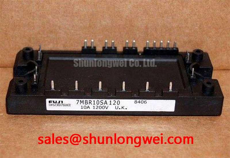
Fuji Electric 7MBR10UF120 1200V 10A PIM Power Module
Begin field replacement checks with the equipment isolated: inspect the module body and terminals, confirm the nameplate against the required electrical boundary, and compare cold resistance readings with a known good unit before reconnecting the drive. The 7MBR10UF120 is a Fuji Electric power integrated module configured as a 7-pack PIM, combining an integrated rectifier and brake stage with an IGBT inverter section for compact industrial drive architectures.
At a case temperature of Tc = 25°C, the supplied factory specification identifies a 1200 V collector-emitter voltage rating, a 10 A collector current rating, and a typical Vce(sat) of 2.10 V. The specified switching capability is up to 20 kHz. These values are official specification data supplied for this product page; they should not be treated as a complete substitute for the original Fuji Electric datasheet, application limits, switching waveforms, or thermal curves.
| Parameter | Official Specification | Engineering Significance |
|---|---|---|
| Manufacturer | Fuji Electric | Confirm the original drive documentation and terminal arrangement before service replacement. |
| Configuration | 7-pack PIM | Integrates rectifier and brake functions with the power switching stage. |
| Collector-emitter voltage, Vces | 1200 V at Tc = 25°C | Supports evaluation in drive systems connected to 400 V to 480 V AC input classes, subject to the complete system design. |
| Collector current, Ic | 10 A at Tc = 25°C | Relevant to current loading in compact automation and servo drive applications. |
| Typical saturation voltage, Vce(sat) | 2.10 V | Used when estimating conduction loss together with actual current, duty cycle, and case temperature. |
| Switching frequency | Up to 20 kHz | Allows evaluation for quiet motor operation and compact filtering, with switching loss verified at the system level. |
Fuji Electric describes PIM products as integrated power semiconductor assemblies. Engineers reviewing the internal topology can consult the Fuji Electric PIM product reference. The external product page for this component is available at 7MBR10UF120.
7MBR10UF120 Circuit Protection and Reliability: Isolated DC DC Supply Verification
When this PIM is installed in a CNC or robot servo drive, the gate driver supply and control electronics should be checked as part of the replacement procedure rather than treated as separate service items. Verify the isolation architecture required by the original drive documentation, including the isolation barrier, insulation coordination, creepage, clearance, and transient behavior of the selected DC DC converter. The supplied product information does not establish a specific isolation voltage or common-mode transient immunity value for the complete gate-driver circuit, so those limits remain system design requirements.
Gate-driver power should reach the intended operating state before switching commands are enabled. Designers should verify the actual power-up and power-down sequence, undervoltage lockout behavior, fault reset timing, and the reference potential used by each high-side and low-side channel. A control board that appears functional at low voltage can still produce unwanted gate activity if the isolated supply collapses during acceleration, regenerative braking, or a short-duration line disturbance.
For a field inspection, disconnect the motor and DC bus, discharge stored energy according to the equipment service procedure, and inspect the driver-side supply under controlled power-up. Compare each gate signal with the corresponding emitter reference using suitable differential measurement equipment. Unexpected pulses, unequal amplitudes, or timing movement between channels may indicate a grounding, isolation, driver supply, or layout problem; verify the signal path against a known-good axis before attributing the behavior to the power module.
Minimize the physical area of the gate-drive loop and keep power commutation paths separate from sensitive control wiring. Clearance around the high-voltage terminals must follow the system insulation design and applicable equipment standard. The 1200 V rating of the device does not independently certify the finished drive for insulation, EMC, or safety compliance. The complete assembly remains responsible for those evaluations.
For applications that require a different current class or a broader comparison during service planning, engineers may review the objectively related 7MBR50SB120-01. This is a separate device and must be checked against the original mechanical, electrical, gate-drive, and protection requirements rather than assumed to be a direct substitute.
7MBR10UF120 Thermal-Electrical Optimization: Gate Damping and Miller Control
The stated switching capability of up to 20 kHz makes gate-loop behavior important in compact servo inverters, but operating frequency alone does not define safe switching performance. Actual switching loss depends on gate resistance, driver strength, DC-link voltage, load current, commutation layout, junction temperature, and the selected switching pattern. These factors should be measured together during commissioning.
When high dv/dt operation produces unwanted movement on the complementary gate signal, the design team should first examine the complete gate loop. A short, low-impedance connection between driver and module gate terminals helps limit the voltage generated by stray inductance. Gate damping can be introduced as a typical starting point during bench tuning, then adjusted from measured rise time, overshoot, switching loss, and device temperature. A value should not be presented as a fixed factory requirement for this module because the appropriate setting belongs to the gate-driver and layout combination.
Active Miller clamp circuitry can be considered where the gate-driver architecture supports it. Its purpose is to hold the inactive device in a controlled state while the complementary device changes voltage rapidly. Designers should verify clamp activation thresholds, propagation delay, driver current capability, and the reference connection at the module terminals. Negative gate bias is also a system-level design consideration, not an official specification identified in the supplied product data. Any negative bias level must be verified against the driver, insulation, gate-emitter limits, and the original Fuji Electric application documentation.
Dead time should be established from measured turn-off and turn-on behavior, including driver delay, temperature variation, current direction, and reverse-recovery interaction in the commutation path. Too little interval can increase cross-conduction risk, while excessive interval can increase diode conduction and distortion. Use complementary gate interlock logic, monitor both channels simultaneously, and validate the final timing under the actual motor and DC-link conditions.
Parallel operation requires separate verification of static and dynamic current sharing. A positive temperature coefficient may assist current balancing in some operating regions, but it should not be assumed without the relevant electrical curves and thermal conditions. If multiple power paths are evaluated, match the external conductors, gate-drive timing, thermal interfaces, and current measurement locations, then confirm sharing during startup, acceleration, deceleration, and regenerative braking.
7MBR10UF120 Operational Boundaries: DC Bus and Low-Inductance Commutation
Inspect the DC-link path before commissioning a replacement module. Check busbar joints, laminated conductor interfaces, capacitor connections, brake chopper wiring, and the physical symmetry of the positive and negative current paths. A loose joint, damaged insulator, or altered busbar route can change commutation behavior even when the replacement module has the correct voltage and current ratings.
The basic switching relationship is that the peak device voltage rises with the DC-bus voltage and the product of stray inductance and current slew rate. This engineering calculation is useful for interpreting oscilloscope measurements, but it does not provide a universal voltage limit or a fixed busbar dimension for the 7MBR10UF120. The system engineer must determine the allowable peak by comparing measured switching overshoot with the module rating, operating temperature, protection response, and the complete drive safety margin.
Use a compact, symmetrical commutation loop and place the local high-frequency DC-link capacitance according to the original power-stage layout. Snubber selection is also system determined. A capacitor that is too small may not control the measured overshoot, while excessive capacitance can increase pulse current and switching loss. Evaluate the snubber with the actual busbar, capacitor ESL, switching frequency, load current, and braking sequence rather than selecting it from voltage rating alone.
The integrated brake stage is relevant when the servo drive absorbs regenerative energy during rapid deceleration. The braking resistor, chopper control, thermal protection, and duty profile must be reviewed as one energy path. The 10 A collector-current specification does not define the permissible brake-resistor energy, pulse duration, or enclosure cooling requirement. Those values must come from the drive manufacturer’s system documentation and measured operating conditions.
In the upstream power path, the related 7MBR50SA120-50 may be evaluated as a separate rectifier or complementary-stage reference. It should not be treated as an automatic pairing or replacement. Confirm the rectifier current, surge behavior, bus precharge arrangement, brake topology, and mechanical interface before modifying the drive.
Maintenance Note: Clean the heatsink and airflow path routinely, inspect thermal-interface material for aging, and trend terminal or case temperature under a repeatable load before returning the axis to production.
Field Diagnostics and Commissioning: Junction-to-Case Thermal Evaluation
Thermal commissioning should begin with the actual mounting condition. Confirm that the heatsink surface is clean and flat, the interface material is applied consistently, and the module sits without mechanical distortion. Verify terminal tightness using the equipment manufacturer’s specified procedure rather than assigning an unverified torque value to this particular module.
The supplied data gives Vce(sat) typical = 2.10 V at Tc = 25°C. This figure can support an initial conduction-loss estimate when multiplied by measured current and the relevant duty interval, but the result is not a complete junction-temperature calculation. Switching loss, diode behavior, brake operation, thermal-interface resistance, heatsink airflow, ambient temperature, and transient loading must also be included. Use the manufacturer’s thermal curves and transient impedance data where available.
For pulsed overload investigation, record collector current, DC-link voltage, gate voltage, case temperature, and switching waveforms at the same operating point. A multi-section RC thermal model can then be compared with measured case-temperature response to estimate junction movement over time. This is an engineering calculation, not a field-life prediction. Without an authoritative test report, no specific lifetime, failure rate, or overload recovery window should be assigned to the product.
If the module trips during acceleration or braking, inspect the complete evidence set: fault history, phase-current balance, gate timing, bus voltage, heatsink temperature, fan condition, and mechanical load. A single symptom may have several contributing paths. Compare the affected axis with an operating axis under equivalent conditions, and use a differential probe and properly rated current probe to avoid introducing a measurement fault.
After replacement, commission at reduced mechanical demand while monitoring the three phase outputs and the brake sequence. Increase operating demand only after confirming stable gate timing, acceptable voltage overshoot, balanced current, and a repeatable thermal response. For broader maintenance procedures covering measurement discipline and failure analysis, consult the Field Engineer’s Handbook.
The 7MBR10UF120 can therefore be evaluated for high-dynamics multi-axis CNC and robotics servo systems where its 1200 V voltage class, 10 A current rating, 2.10 V typical saturation voltage, up to 20 kHz switching capability, and 7-pack PIM configuration match the original drive architecture. Final acceptance remains dependent on measured electrical stress, thermal performance, isolation design, and the equipment manufacturer’s service requirements.