Content last revised on October 20, 2026
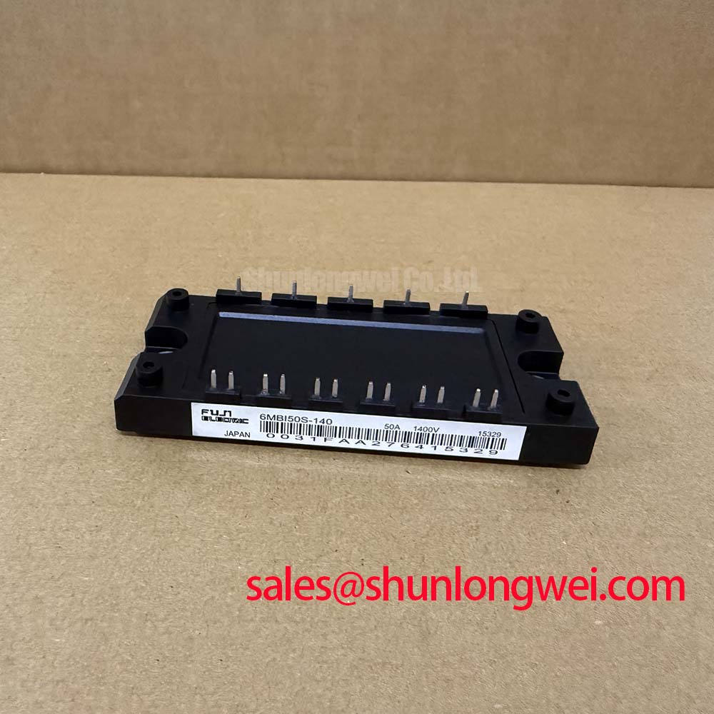
With the inverter isolated, record the cold terminal condition of the failed power stage before removing the module, then compare the measured phase paths with a known-good assembly. For the Fuji Electric 7MBR35SB140_0105, the supplied factory ratings are 1400.0 V and 35.0 A, with a Fuji Power Module housing. These are Official Specification values for identification and replacement screening, not a complete switching or thermal operating profile.
On a compact industrial inverter or high-speed CNC spindle drive, first confirm the original bus arrangement, phase-terminal order, gate-drive interface, snubber network, and mounting footprint. A module with the same voltage and current label still requires circuit-level compatibility checks because gate timing, protection thresholds, isolation construction, and mechanical heat transfer are determined by the complete assembly.
Assembly Integrity and Layout Architecture for the Fuji Electric 7MBR35SB140_0105
Isolation integrity should be checked before any powered test. Disconnect the gate-drive board and auxiliary wiring, discharge the DC link using the equipment manufacturer’s approved procedure, and inspect the terminal area for carbon tracking, metal dust, loose hardware, and contamination paths. The test objective is to ensure that the power terminals, control reference, and baseplate remain separated under the equipment’s applied electrical stress.
Reinforced galvanic isolation and common-mode transient behavior are Design Considerations for the surrounding gate-drive system rather than specifications established by the three supplied product values. If the drive architecture relies on an isolation barrier above 5 kV or a common-mode transient immunity level above 100 kV/µs, the isolation device, gate-driver board, module construction, and test method must be assessed together. Do not assign those figures to the 7MBR35SB140_0105 without the applicable manufacturer datasheet or test report.
During an intermittent trip, monitor the gate-to-emitter signal at the module terminals rather than only at the driver output. A short, unwanted pulse can be created by common-mode displacement current, reference bounce, or parasitic coupling around the power loop. The practical layout response is to keep the gate-drive return physically close to its corresponding emitter return, separate high-current commutation paths from sensitive control wiring, and avoid routing the gate signal alongside fast collector-current conductors for long parallel distances.
Clearance and creepage must be reviewed against the actual working voltage, pollution level, altitude, enclosure condition, and applicable equipment standard. Airborne dust in a CNC cabinet can combine with condensation and flux residue to create a surface leakage path that is not visible during a quick visual inspection. Clean the board and module surroundings using a process approved for the equipment, then repeat the insulation and functional checks after the surface has dried.
High-altitude installations also deserve a separate Design Consideration. Reduced air density can alter external insulation performance, while cosmic-ray exposure can influence the statistical risk assessment of high-voltage switching devices. FIT, single-event burnout, and altitude derating figures require a defined device technology, operating profile, environmental model, and authoritative source. They should not be inferred from the 1400.0 V label or presented as field-life predictions for this module.
For practical service documentation, record the module rating, the original gate-driver board revision, terminal photographs, measured isolation results, and the DC-link protection arrangement. The linked Field Engineer’s Handbook provides a useful reference point for organizing test evidence and failure-analysis observations without confusing a repair measurement with an official product guarantee.
Transient Dynamics and Electrical Design: Isolation and Fault Clearing
When an insulation tester is used, connect it only according to the module and equipment service procedure, with all sensitive gate-drive electronics disconnected. A Design Consideration for this class of assembly is terminal-to-baseplate insulation screening at 500 MΩ or greater when tested at 2.5 kV DC, where that test level is required by the applicable equipment documentation. Treat this as an integration test criterion, not as an unverified factory specification for the 7MBR35SB140_0105.
A falling insulation result should prompt a structured review of the module surface, mounting interface, thermal compound contamination, terminal washers, fastener debris, and the surrounding carrier board. A ceramic substrate or baseplate path can be affected by mechanical stress, contamination, or local discharge activity. Do not identify a microscopic ceramic crack from an insulation reading alone; correlate the result with visual evidence, repeated controlled measurements, and the module’s service history.
Mechanical flatness matters because uneven clamping can stress the power assembly while also degrading heat transfer. Remove old compound completely, inspect the contact surface for burrs, and apply the approved thermal interface material as a uniform thin layer. The required fastener sequence and torque must follow the equipment or module assembly documentation, since the correct value depends on the screw size, washer arrangement, baseplate design, and heat sink material.
⚠️ Field Alert: Never insert or remove the gate-drive connector while the DC link or auxiliary control supply is energized.
Fault clearing should be coordinated with the module’s surge capability and the protective device’s I²t behavior. A high-speed semiconductor fuse must interrupt the fault before the module is exposed to destructive energy, but fuse selection cannot be made from the 35.0 A nominal rating alone. Compare the actual fuse clearing curve, prospective fault current, DC-link capacitance, wiring impedance, and the device’s published short-circuit or surge limits. The Mersen Protistor® High Speed Semiconductor Protection Fuses resource is a suitable industry reference for fuse technology and coordination principles.
For a front-end arrangement that includes a separate rectifier or braking stage, review the complete energy path rather than treating the IGBT module as an isolated replacement. The 7MBI100U4E-120 can be examined as a neutral reference for a related power-stage discussion, but its electrical role, pin arrangement, and ratings must not be assumed to match the installed circuit. Check the original schematic and the board’s protection logic before connecting any associated device.
When switching edges produce unexplained trips, use a differential probe and a controlled low-energy test condition to observe collector-emitter voltage, gate-emitter voltage, and the gate-driver return. Look for overshoot, ringing, delayed turn-off, or a gate waveform that changes when the DC-link wiring is repositioned. These observations can distinguish a layout or driver interaction from an insulation problem without assigning a single cause from one symptom.
| Device reference | Category | Published identification values | Replacement review point |
|---|---|---|---|
| 7MBR35SB140_0105 | Fuji Power Module | 1400.0 V, 35.0 A | Confirm terminal arrangement, gate-drive conditions, mechanical fit, protection coordination, and thermal interface |
| 7MBR100SB060-50 | Related Fuji module reference | Consult its product documentation | Use only as a comparison reference; do not assume electrical or mechanical interchangeability |
7MBR35SB140_0105 Circuit Protection and Reliability: Gate Resistance, Miller Control, and Switching Dissipation
When a modern IGBT module is placed on a legacy drive board, begin gate-resistor calibration with the existing external network documented. Separate turn-on and turn-off paths where the driver design permits, then inspect the gate waveform at the module pins under the same supply, load, and wiring arrangement used by the original assembly. The purpose is to balance switching loss, electromagnetic ringing, gate overstress, and fault-response timing rather than to apply a universal resistor value.
The Miller plateau is the point at which gate current is diverted into changing collector-emitter voltage. The effective transfer depends on gate charge, collector current, DC-link voltage, temperature, driver impedance, and the module’s collector-gate capacitance. A larger Miller-related capacitance can increase the current required to hold the gate stable during a fast voltage transition. An active Miller clamp or an appropriate negative-bias arrangement may help suppress unwanted turn-on, but the clamp threshold, driver supply limits, isolation behavior, and module gate-emitter rating must be verified as a complete design.
For bench tuning, use a conservative initial gate-drive condition and change one variable at a time. Compare turn-on and turn-off waveforms at the module terminals, then check switching dissipation through the system’s approved thermal and electrical test method. If the gate resistor is reduced, switching may become faster while voltage overshoot and ringing become more sensitive to stray inductance. If it is increased, switching stress may reduce in one area while heat generation and fault-clearing delay increase elsewhere.
Gate-loop parasitic inductance should be minimized to suppress oscillation and turn-off overshoot. Keep the driver output, gate resistor, gate terminal, and emitter return within a compact loop, and avoid sharing the gate return with a high-current emitter path unless the circuit was specifically designed for that arrangement. The final layout must be verified with measured gate voltage and collector-emitter voltage during switching tests, with peak values checked against the applicable device and driver limits.
Active clamping is a system protection technique, not a substitute for correct gate timing or DC-link control. During a high-voltage transient, the clamp response depends on sensing location, propagation delay, clamp current capability, gate-driver impedance, and the energy available in the commutation loop. Validate the protection response under the actual fault and load conditions used by the compact inverter or CNC spindle drive. Do not describe a clamp as sufficient solely because it is present on the schematic.
Legacy boards may also contain gate-emitter resistors, desaturation detection, soft shutdown, dead-time generation, and interlock logic that were tuned for a different module family. Check whether the replacement device reaches the expected gate plateau and whether the driver can source and sink the required current without abnormal supply droop. A mismatch can appear as excess heat, intermittent overcurrent protection, or irregular phase current, so compare all three phase legs and not only the leg associated with the original failure.
For applications evaluating newer wide-bandgap switching stages, the Wolfspeed Silicon Carbide power module materials illustrate why switching speed, gate-loop construction, protection response, and electromagnetic compatibility must be treated as a coordinated design problem. That reference is not a substitute for the Fuji Electric module data or a direct replacement recommendation.
The 7MBR35SB140_0105 remains identified here by its supplied Official Specification values of 1400.0 V, 35.0 A, and Fuji Power Module package category. Before returning a repaired inverter to service, confirm the original terminal mapping, isolation test procedure, gate-drive compatibility, protective fuse coordination, heat-sink contact, and switching waveform under controlled conditions.