Content last revised on September 10, 2026
Diagnostic and Engineering Analysis of the 7MBR75U2B060-50 Power Integrated Module in Heavy-Duty VFD Applications
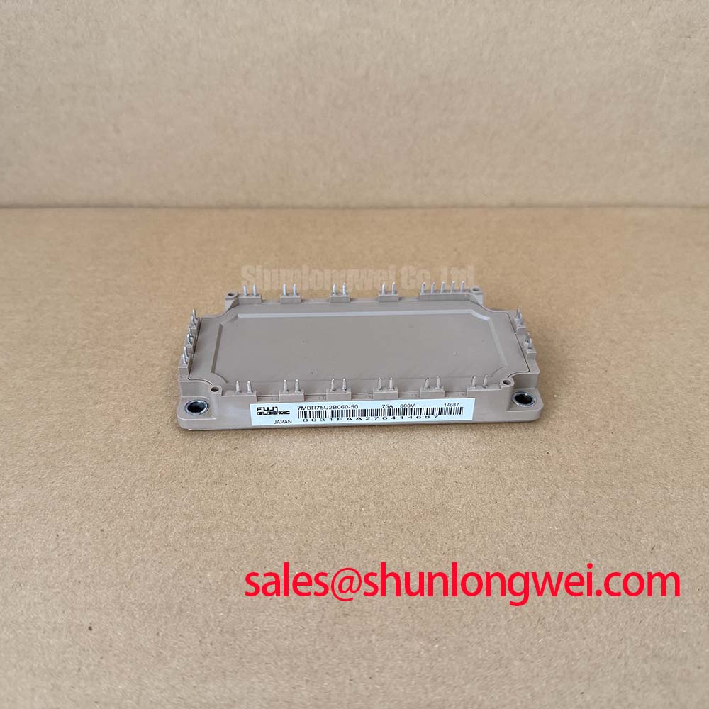
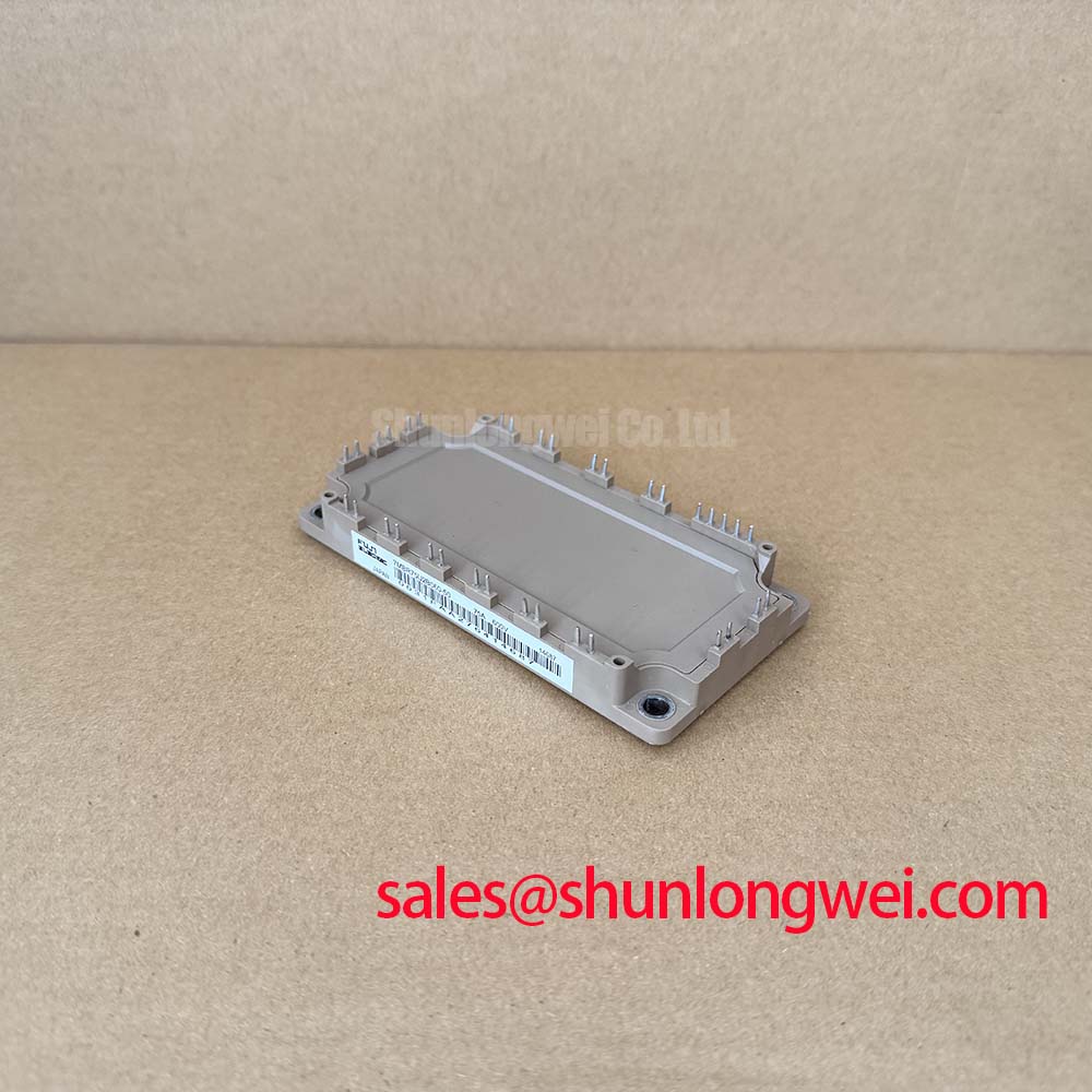
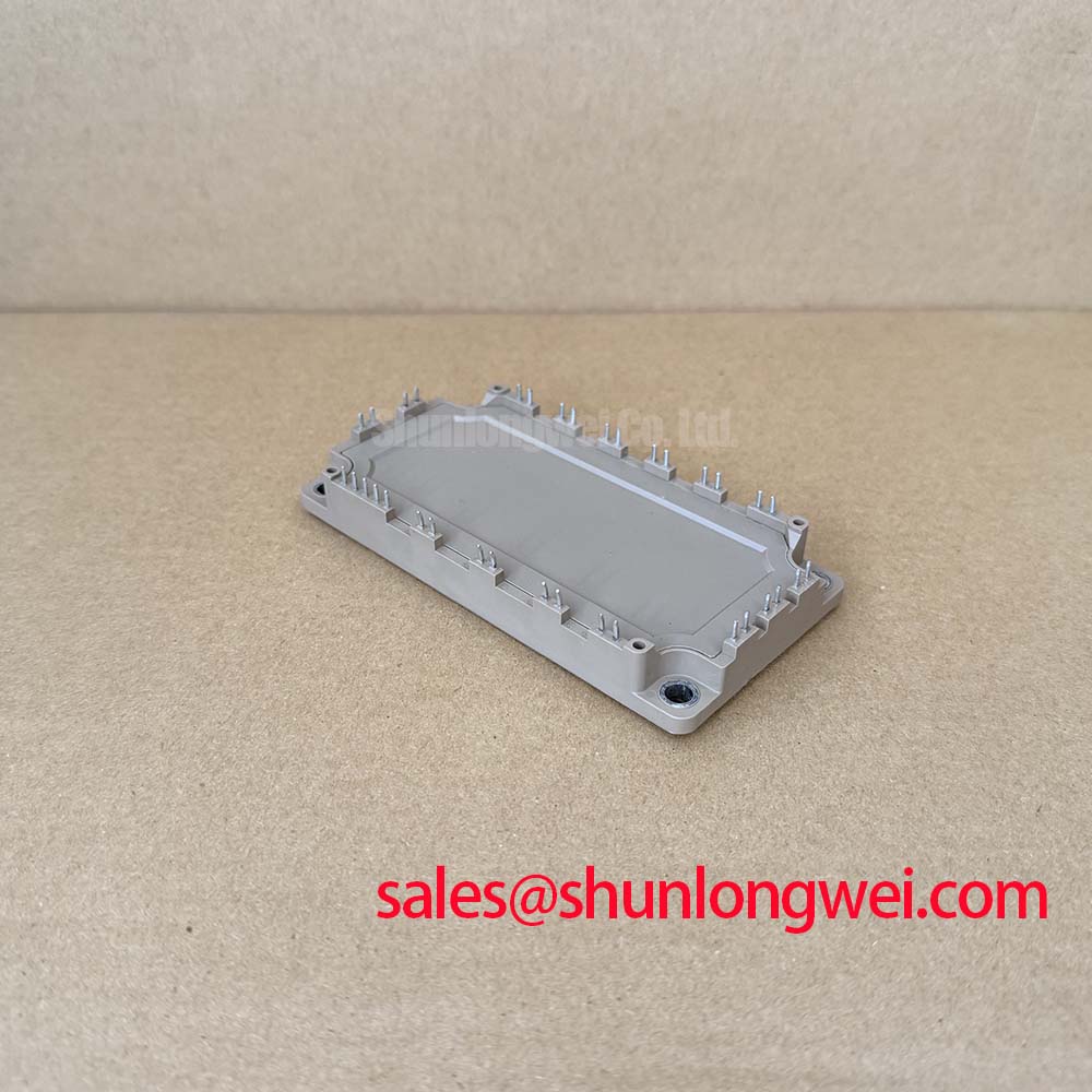
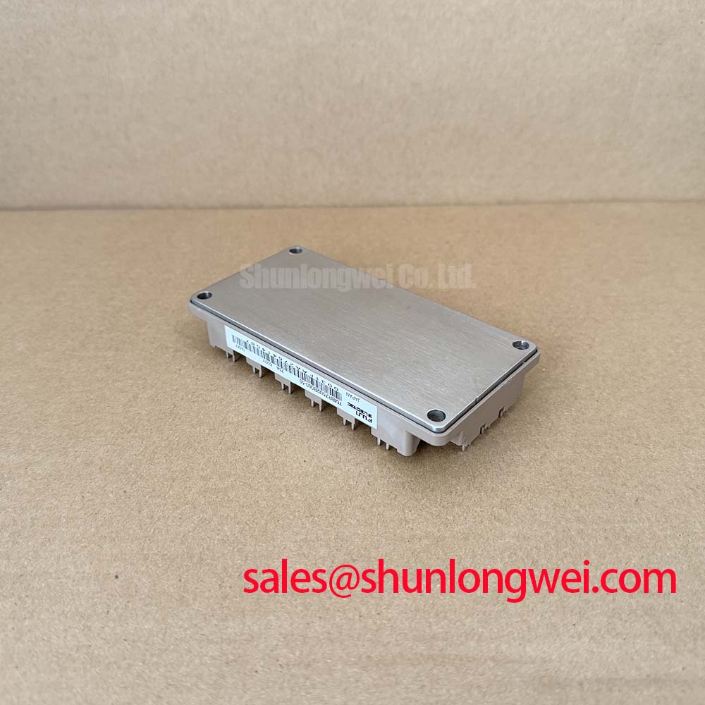
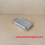
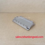
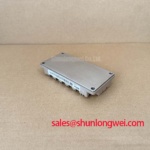
When an industrial variable frequency drive (VFD) trips under heavy plant loading, field service personnel face immediate operational pressure to isolate the root cause and restore uptime. The 7MBR75U2B060-50 from Fuji Electric is a Power Integrated Module (PIM) architecture widely deployed across three-phase motor drives, material handling machinery, and industrial automation converters. Integrating a three-phase diode bridge rectifier, a dynamic braking chopper stage, and a three-phase IGBT inverter bridge into a compact footprint, this module condenses complex power flow into a single mechanical housing.
In high-torque variable frequency motor drive installations, power semiconductors face repetitive thermal cycling, steep turn-off voltage transients, and unpredictable motor-side ground faults. Evaluating replacement components and executing rapid bench triage demands a rigorous understanding of the module's ratings, thermal metrics, and internal topology. The 7MBR75U2B060-50 specifies an inverter stage rated at VCES = 600V and continuous collector current IC = 75A at a case temperature of 25°C, with a typical saturation voltage VCE(sat) = 2.2V (Official Datasheet Specification). The integrated input rectifier handles repetitive peak reverse voltages up to VRRM = 800V with an average output current rating IO = 75A, while the dedicated dynamic brake switch is rated at VCES = 600V and IC = 30A (Official Datasheet Specification).
| Functional Section | Key Electrical Parameter | Maximum Rating / Typical Value | Operational Unit |
|---|---|---|---|
| Inverter IGBT Stage | Collector-Emitter Breakdown Voltage (VCES) | 600 | V |
| Inverter IGBT Stage | Continuous Collector Current (IC @ Tc = 25°C) | 75 | A |
| Inverter IGBT Stage | Saturation Voltage (VCE(sat) typ @ Tj = 25°C) | 2.2 | V |
| Inverter Thermal Boundary | IGBT Junction-to-Case Thermal Resistance (Rth(j-c) max) | 0.49 | °C/W |
| Inverter Thermal Boundary | FWD Diode Junction-to-Case Thermal Resistance (Rth(j-c) max) | 0.79 | °C/W |
| Brake Chopper Section | Collector-Emitter Breakdown Voltage (VCES) | 600 | V |
| Brake Chopper Section | Brake Collector Current (IC) | 30 | A |
| Brake Thermal Boundary | Brake IGBT Junction-to-Case Thermal Resistance (Rth(j-c) max) | 0.94 | °C/W |
| Input Converter Section | Repetitive Peak Reverse Voltage (VRRM) | 800 | V |
| Input Converter Section | Rectified Average Output Current (IO) | 75 | A |
| Module Isolation | Dielectric Insulation Withstand (Viso, 1 minute) | 2500 | V AC |
When executing an emergency cold-check on a damaged VFD using a digital multimeter in diode mode, field technicians must verify the health of all three stages prior to installing a replacement. A defective free-wheeling diode (FWD) or a punctured gate-emitter oxide layer will exhibit dead shorts or anomalous forward voltage drops (nominal healthy drops sit between 0.35V and 0.55V across the diodes). Systemic verification against the Field Engineer’s Handbook provides standardized pass/fail thresholds for gate leakage and collector isolation before re-energizing the DC bus.
DC-Link Capacitance Bank Layout and Low-ESL Busbar Interconnection Techniques
Heavy-duty AC motor drives operate under continuous high-frequency pulse-width modulation (PWM), switching inductive motor currents across inductive DC distribution links. During rapid IGBT turn-off transitions, the rate of current decay (di/dt) interacts directly with the total loop stray inductance between the DC-link capacitor bank and the module terminals. The resulting inductive turn-off spike adds directly onto the steady-state DC bus voltage, where the transient peak voltage across the collector-emitter terminals equals the sum of the DC link voltage and the product of stray loop inductance and turn-off di/dt. In a 600V-rated power module such as the 7MBR75U2B060-50, maintaining a total stray inductance below 25nH is essential to keep high-frequency overshoots safely below the collector-emitter breakdown threshold under peak fault trip conditions.
Achieving this low parasitic inductance requires planar, laminated busbar geometry. By stacking the positive (P) and negative (N) copper bus planes in close proximity separated only by a thin dielectric film (such as 0.25mm to 0.5mm Nomex or Kapton), the magnetic fields generated by opposing currents cancel each other out effectively. Traditional point-to-point discrete wire harnesses or non-laminated copper bars introduce 50nH to 120nH of loop inductance, generating excessive voltage overshoot during hard turn-off at full 75A current load, often precipitating avalanche breakdown of the silicon die.
High-frequency film snubber capacitors (polypropylene dielectric, low Equivalent Series Inductance) must be mounted directly across the P and N terminal pins of the 7MBR75U2B060-50. Placing the snubber capacitor within 15mm of the physical power terminals absorbs the high-frequency commutation energy without allowing transient voltage ringing to couple back into the electrolytic reservoir bank. For broader system topologies and converter configurations, reference material on Switched-Mode Power Supply (SMPS) Topologies and Conversion illustrates the baseline decoupling architecture required across intermediate DC links.
⚠️ Field Alert: When re-assembling the module onto the drive heatsink, the mechanical mounting sequence dictates long-term thermal reliability. Uneven bolt tensioning warps the internal Direct Copper Bonded (DCB) ceramic substrate, creating micro-fractures in the thermal interface layer. Apply thermal paste in a controlled 80–100 µm stencil layer and torque the M5 chassis bolts progressively to 2.5–3.5 N·m (General Industry Design Consideration for M5 fasteners) using a cross-pattern sequence. Never fully torque one screw while the opposing corner is loose.
Mitigating Hard Switching Transients via Active Desaturation Soft Shutdown
Industrial motor drives present severe operating hazards, including output cable flashovers, terminal phase-to-phase shorts, and stator insulation breakdown. Under a Type-I (fault established prior to turn-on) or Type-II (fault occurring while the device is in conduction) short-circuit event, the collector current through the 7MBR75U2B060-50 surges rapidly to several times its continuous 75A rating. The device enters desaturation: the collector-emitter voltage collapses out of saturation and rises toward the DC bus potential while conducting massive short-circuit currents. According to Short-Circuit Safe Operating Area (SCSOA) operational boundaries, the module must detect and interrupt this fault state within 10 µs at rated junction temperatures to prevent thermal explosion.
Directly clamping or abruptly pulling down the gate voltage during a 300A+ short-circuit interruption induces a destructive turn-off di/dt, generating a massive transient voltage spike that ruptures the 600V silicon die. Driver boards must employ Active Desaturation Detection coupled with Two-Stage Turn-Off (Soft Shutdown). The desaturation detection network uses a high-voltage blocking diode connected to the collector terminal, monitoring VCE through a dedicated blanking filter (typical blanking time: 1.5 µs to 2.5 µs to avoid false tripping on standard turn-on transients).
When the sensing threshold (typically 6.5V to 7.5V) is exceeded, the driver circuit immediately decouples the hard gate pulldown resistor and routes the gate discharge current through a secondary, high-impedance soft-turn-off resistor (such as 47 Ω to 100 Ω, representing a Typical Starting Point for bench tuning). This engineered reduction in gate voltage discharge rate slows down the current ramp, safely dissipating the inductive stored energy and preserving the module within its rated transient envelope.
Technicians troubleshooting recurring drive trips should check the gate-emitter drive boards for cracked surface-mount desat sensing diodes, open-circuit gate clamping zener diodes, or carbon tracking around the module's small-signal control pins. Inspecting physical creepage and clearance distances across the driver isolation barrier prevents ground bounce noise from inadvertently triggering false desaturation faults during high-load motor acceleration.
Cosmic Ray Robustness: Voltage Derating Curves across 2000m-4000m Altitudes
Standard power converter reliability metrics assume sea-level atmospheric pressures and standard environmental conditions. When variable frequency drives containing the 7MBR75U2B060-50 are deployed in high-altitude mining sites, alpine pumping stations, or plateau industrial plants at elevations between 2000m and 4000m above sea level, two primary physical degradation mechanisms accelerate: reduced convective cooling efficiency due to lower air density, and increased susceptibility to Single Event Burnout (SEB) driven by high-energy terrestrial neutron flux.
Atmospheric neutron flux increases substantially with altitude. High-energy neutrons colliding with the silicon lattice of a reverse-biased IGBT generate localized electron-hole plasma filaments. If the applied DC-bus electric field across the drift region is sufficiently intense, this microscopic avalanche can cascade into an unrecoverable thermal runaway path, permanently shorting the collector to the emitter without any prior thermal warning. The Failure in Time (FIT) rate for cosmic ray-induced SEB exhibits an exponential relationship with the steady-state collector-emitter operating voltage.
For installations utilizing 600V-class modules like the 7MBR75U2B060-50 at high elevations, engineering best practice requires voltage derating curves to maintain target reliability. At an altitude of 3000m, keeping the continuous DC-bus voltage clamped under 380V–400V DC provides the necessary voltage headroom to reduce cosmic-ray SEB failure probability down to baseline sea-level equivalents (General Industry Design Consideration). Furthermore, air clearance and creepage distances must be recalculated using altitude correction factors according to IEC 60664-1, as dielectric breakdown of air occurs at lower peak voltages in thin atmospheres. When replacing damaged hardware in highland facilities, engineers should inspect surge arrestors and Metal Oxide Varistors (MOVs) to verify that transient grid line surges are aggressively attenuated before reaching the DC link.
For broader parametric verifications and package variant references, technical literature accessible via the Fuji Electric Power Semiconductors Portal details the standard mechanical outlines and baseplate insulation profiles across the manufacturer's medium-power line.
Symmetrical Busbar Geometry for High-Current Parallel Module Arrays
When high-output industrial drives require current capacities exceeding the 75A capability of a single 7MBR75U2B060-50, design engineers may configure multiple power stages or inverter legs in parallel. Achieving uniform current sharing among parallel modules requires balancing both static (conduction) and dynamic (switching) operating phases.
Static current sharing relies on the positive temperature coefficient of the IGBT's saturation voltage VCE(sat) at nominal and elevated operating currents. When two or more IGBT dice conduct in parallel, the die handling higher instantaneous current dissipates more thermal energy. As its junction temperature rises, its internal VCE(sat) increases (exhibiting a positive temperature coefficient in the rated conduction regime), naturally forcing excess current into the cooler companion device. This self-balancing mechanism stabilizes steady-state thermal distribution across the inverter channels.
Conversely, dynamic current sharing during turn-on and turn-off transitions is entirely governed by loop symmetry, parasitic inductance balancing, and gate drive matching. A mismatch of only 3nH to 5nH in terminal busbar inductance between parallel paths can cause one module to switch substantially faster than the other, forcing it to absorb the bulk of the switching loss Eon and Eoff. To secure balanced dynamic operation:
- Maintain completely symmetrical busbar trace lengths from the DC link capacitor bank to the P/N input pins of each module.
- Ensure individual, isolated gate drive resistors for each module gate terminal rather than tying multiple gates directly to a single driver output pin, which prevents circulating parasitic gate oscillations.
- Twist gate and emitter control leads tightly together to eliminate magnetic loop pickup from adjacent high-current output phases.
- Incorporate dedicated ferrite beads on gate signal paths to suppress high-frequency ringing caused by gate-emitter capacitance interaction with trace inductance.
During plant overhaul or retrofit campaigns where a different module family or higher voltage class is evaluated for parallel or sub-assembly integration, technicians frequently encounter alternative configurations. For systems requiring higher voltage blocking margins or dedicated single-bridge configurations, the related 6MBI10S-120 offers a 1200V platform for medium-voltage industrial control tiers.
Systematic verification of terminal torque, dynamic gate damping resistors (suggested initial gate damping: 10 Ω, representing a Typical Starting Point for bench tuning), and clean thermal baseplates ensures that field replacements of the 7MBR75U2B060-50 deliver stable, long-term performance across harsh motor drive environments.