Content last revised on September 10, 2026
Fuji Electric 1MBI600U2A-060-50: Technical Overview & Engineering Analysis
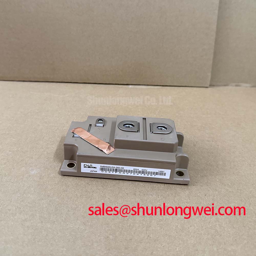
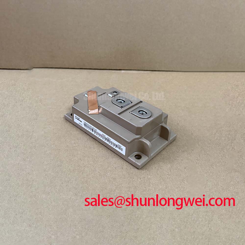
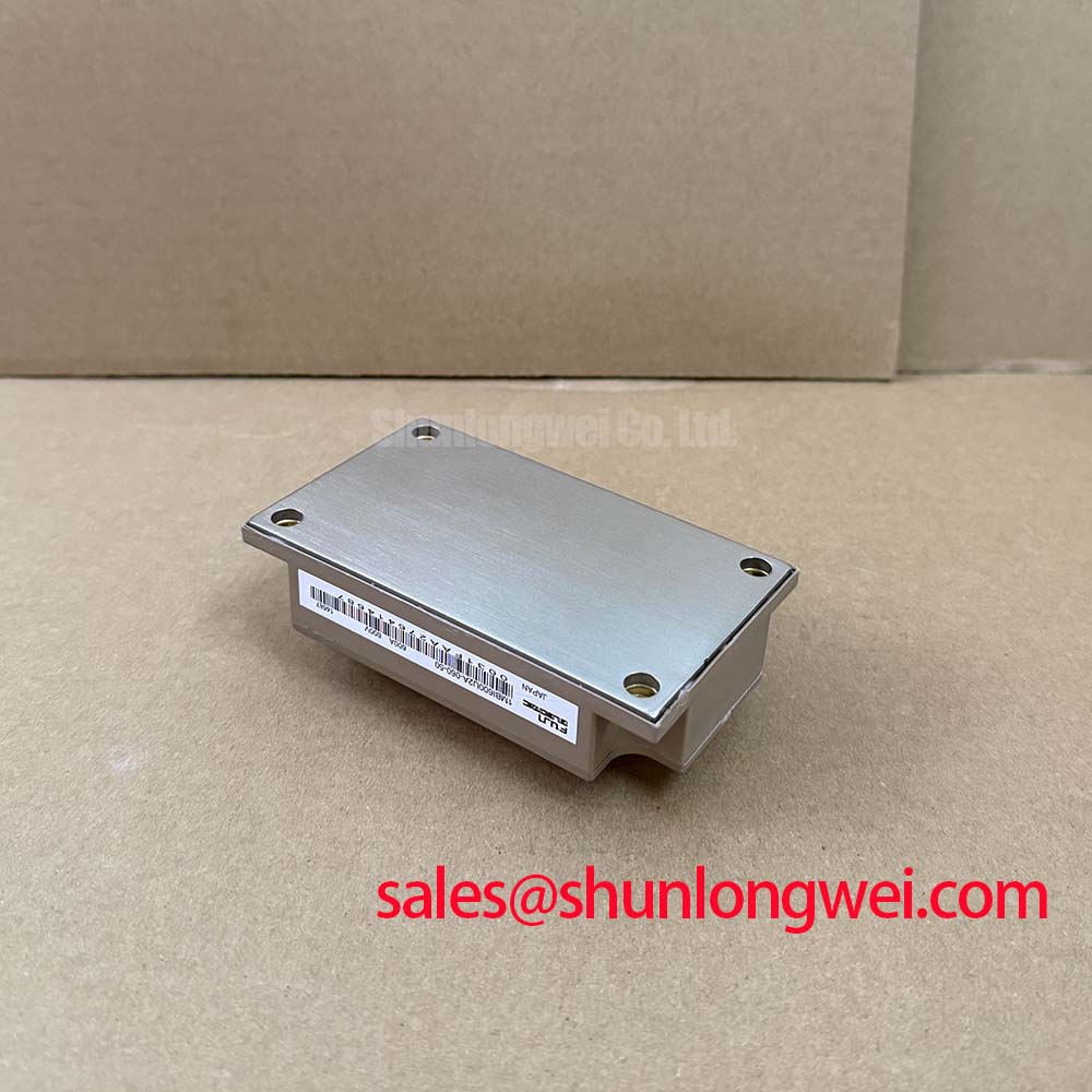
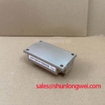
In utility-scale centralized battery energy storage system (BESS) power conversion systems (PCS), power semiconductors experience rigorous thermal cycling, high-current bidirectional power flow, and continuous switching stress. The 1MBI600U2A-060-50 is a high-power single IGBT module manufactured by Fuji Electric, engineered to handle sustained heavy-load commutation in low-voltage, high-current inverter stages and DC-DC bidirectional converters.
From an operations and plant maintenance perspective, understanding the module's electrical boundaries and mechanical assembly requirements is essential for maximizing uptime and preventing catastrophic field failures. The key factory parameters for the 1MBI600U2A-060-50 are summarized below:
| Parameter Symbol | Technical Specification Description | Value / Rating |
|---|---|---|
| VCES | Collector-Emitter Voltage (Maximum Blocking Voltage) | 600 V (Official Datasheet Specification) |
| IC | Continuous Collector Current (Tc = 25°C) | 600 A (Official Datasheet Specification) |
| ICP | Pulsed Collector Current (1 ms duration) | 1200 A (Official Datasheet Specification) |
| VGES | Gate-Emitter Voltage (Continuous Limit) | ±20 V (Official Datasheet Specification) |
| VCE(sat) | Collector-Emitter Saturation Voltage (Typical, Tj = 25°C) | 2.1 V (Official Datasheet Specification) |
| Rth(j-c) | Thermal Resistance, Junction-to-Case (IGBT Element) | 0.083 °C/W (Official Datasheet Specification) |
| Tj | Operating Junction Temperature Range | -40 to +150 °C (Official Datasheet Specification) |
Thermal Feedback & V_CE(sat) Positive Temperature Coefficient Equalization
Utility-scale PCS units frequently deploy multiple switches in parallel to achieve megawatt-level transfer capabilities. Under high-current conduction, current imbalance among paralleled dies can trigger localized overheating and thermal runaway. The 1MBI600U2A-060-50 addresses this challenge through its positive temperature coefficient of saturation voltage at nominal operating ranges. When the junction temperature increases, the internal on-state collector-emitter saturation voltage VCE(sat) shifts upward from its 2.1 V nominal base (Official Datasheet Specification at 25°C), naturally forcing excess current into cooler adjacent branches to establish static current equalization.
Static balancing alone does not resolve dynamic switching imbalances. High di/dt transitions require rigorous physical symmetry in the gate drive layout and DC bus connections. Differences in stray gate-loop inductance or asymmetric emitter return paths can induce divergent turn-on and turn-off delays. To mitigate dynamic sharing discrepancies, field service teams must verify that auxiliary Kelvin-emitter terminals are wired directly to driver return tracks, isolating the gate drive reference from the high-current power path.
When inspecting complex bi-directional PCS topologies where multi-stage conversion is implemented, field technicians often encounter complementary dual modules such as the 2MBI450U4N120-50 working in tandem on higher-voltage sub-links. Maintaining uniform gate trace lengths, tightly twisting gate-emitter wiring pairs, and verifying identical series gate resistance across every paralleled branch remain mandatory preventive practices during scheduled bay refurbishments.
Thermal Interface Material (TIM) Thickness Uniformity and Void Minimization
The copper baseplate of high-power modules is engineered with a deliberate convex bow to compensate for mechanical deflection and thermal expansion against flat heatsinks. Applying thermal interface material (TIM) requires precise thickness control. Applying a layer thinner than 50 µm risks dry contact voids due to micro-groove gaps, while exceeding 100 µm introduces excessive bulk thermal impedance that degrades overall heat transfer across the interface.
⚠️ Maintenance Note: During semi-annual thermal imaging inspections, technicians should flag any delta-T across parallel modules exceeding 8°C under equal load. Over extended operating cycles in high-ambient PCS enclosures, siloxane-based thermal grease is subject to pump-out and dry-out phenomena. If replacement is warranted, clean the heatsink surface with isopropyl alcohol, apply fresh compound using a 75 µm stainless steel stencil, and follow a two-step diagonal torque tightening procedure: pre-torque M5 mounting bolts to 1.0 N·m (Design Consideration), followed by a final uniform torque between 2.5 and 3.5 N·m (Design Consideration based on standard M5 mounting specifications).
Thermal stability also depends on gate-driver power integrity. Gate drive power stages must provide adequate charge per switching cycle without voltage sag. Sizing driver bypass capacitors to comfortably exceed the module's total gate charge requirements ensures that gate voltage does not drift below the intended threshold under continuous high-frequency modulation. Detailed diagnostic procedures for evaluating degraded thermal interfaces and baseplate stress can be referenced in the Field Engineer’s Handbook.
Planar Symmetrical Busbar Geometry: Achieving L_sigma < 20nH to Protect Silicon Junctions
At an operational rating of 600 A and a pulsed limit of 1200 A (Official Datasheet Specifications), turn-off current gradients can generate extreme inductive overvoltage spikes. Because the 1MBI600U2A-060-50 has a maximum collector-emitter blocking limit of 600 V, standard utility PCS systems operating at DC link voltages between 350 V and 420 V have limited voltage headroom. Parasitic loop inductance across the DC bus must be controlled to prevent switching spikes from exceeding the safe operating area limit.
Transient turn-off overvoltage across the module terminals is directly proportional to the total stray inductance multiplied by the turn-off di/dt. In high-power layouts, achieving an equivalent loop inductance Lσ of less than 20 nH (Design Consideration for low-inductance converter design) requires a planar laminated busbar structure. Layering wide, ultra-thin positive and negative copper plates separated by thin dielectric insulation facilitates magnetic flux cancellation, minimizing loop area.
Direct-mount low-inductance film snubber capacitors placed physically adjacent to the module collector and emitter terminals provide a local high-frequency clamp, absorbing energy during hard commutation. For utility energy storage platforms upgrading DC bus architectures to higher voltage tiers, selecting a 1200 V rated alternative such as the 1MBI600U-120 provides the necessary blocking margin. For modern power topologies, advanced packaging and high-speed switching benchmarks can be explored through Fuji Electric 7th-Gen X-Series IGBT Modules.
Optocoupler vs Digital Coreless Transformer Isolation in High-Voltage Switching
The control interface linking the central DSP to the gate driver must maintain reinforced galvanic isolation (commonly rated to withstand insulation test voltages exceeding 2.5 kV to 5.0 kV RMS). In central PCS environments where megawatt battery banks interface with distribution grids, steep dv/dt transients generated during switching can breach lower-tier isolation barriers via parasitic capacitive coupling.
Traditional optocouplers utilize light-emitting diodes and phototransistors, which exhibit performance degradation over time due to LED aging, temperature-induced propagation delay drift, and limited common-mode transient immunity (CMTI). In modern utility-grade PCS applications, digital isolation using coreless transformer or capacitive isolation architectures is widely adopted. These solid-state isolation barriers deliver CMTI ratings exceeding 100 kV/µs (Design Consideration for high-noise industrial switching), preventing spurious gate pulses caused by ground bounce or high-voltage displacement currents.
Driver circuitry must also integrate fast desaturation (DESAT) monitoring directly across the C-E terminals. If a load-side short-circuit occurs, the module exits its low-loss saturation region. DESAT detection sensing circuits must initiate a controlled soft turn-off within the short-circuit safe operating area (typically within 10 microseconds) to prevent destructive transient overvoltage on the silicon die. For system designers transitioning between standard silicon IGBT architectures and next-generation fast-switching platforms, reference data on drive requirements is accessible via Fuji Electric Discrete IGBT & SiC MOSFETs.