

Content last revised on September 13, 2026
2MBI600U4N-120-50 Specifications and Installation Context
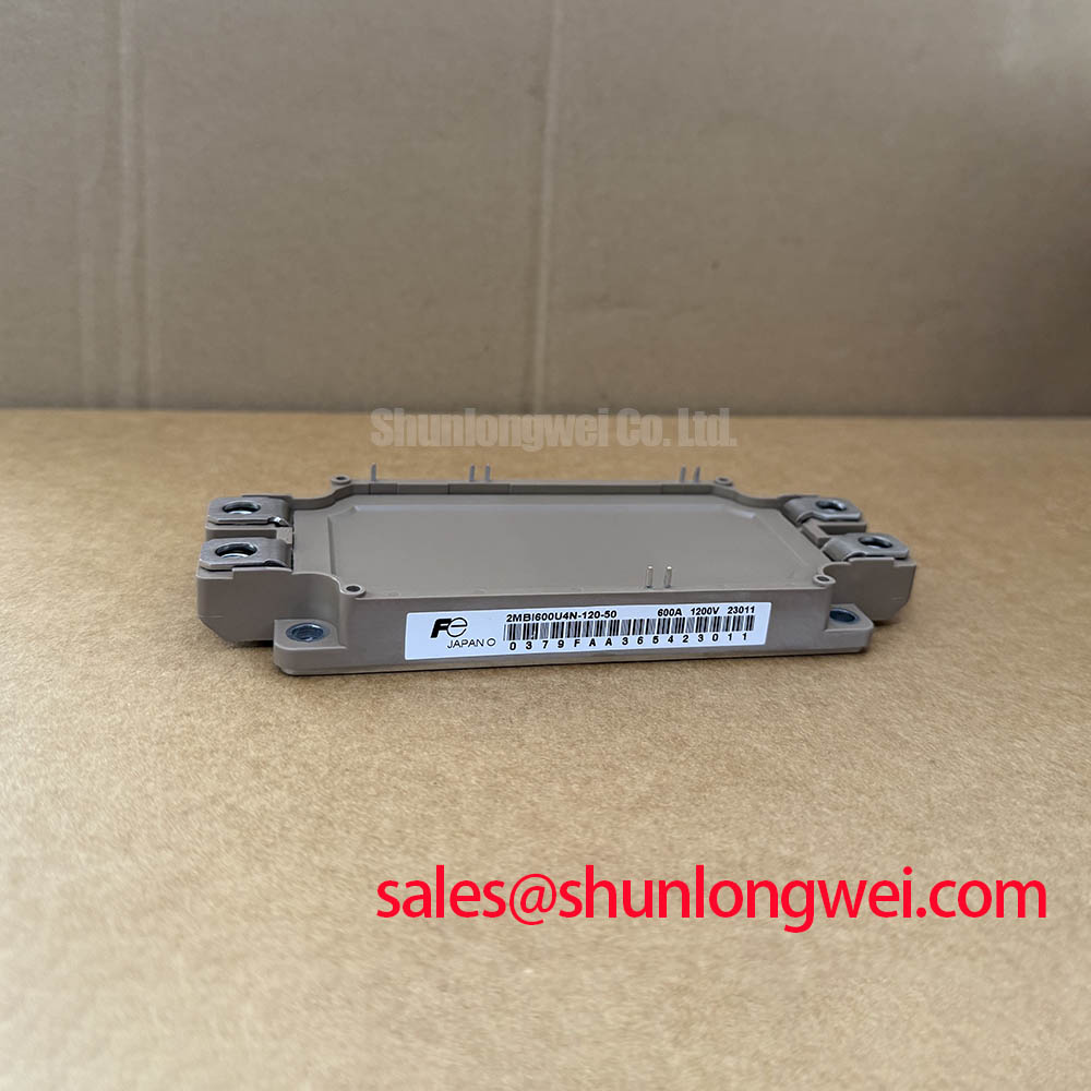
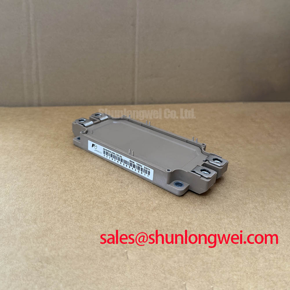
Before connecting the DC bus, verify the terminal identification against the module drawing and compare cold-state gate-to-emitter and power-terminal readings with the removed module’s documented service record. The 2MBI600U4N-120-50 is a Fuji Electric dual IGBT half-bridge module with a specified 1200 V VCES rating and 600 A collector-current rating, both Official Datasheet Specifications. Its dual half-bridge configuration places two switching positions in one package, allowing a compact power-stage arrangement when the surrounding busbar, driver, cooling plate, and protection circuit are designed as one system.
The module’s specified 0.04 °C/W typical junction-to-case thermal resistance supports efficient transfer of heat from the semiconductor junctions to the baseplate interface. This is an Official Datasheet Specification, not a complete thermal-system rating: heatsink performance, interface material condition, clamp distribution, coolant conditions, switching losses, and ambient conditions remain system-determined. The specified 2500 V AC isolation voltage defines the module’s dielectric isolation rating, while enclosure insulation coordination and installation clearances still require verification at equipment level.
| Official specification | Value | Integration relevance |
|---|---|---|
| Collector-emitter voltage, VCES | 1200 V | Voltage-class boundary for switching-device selection |
| Collector current, IC | 600 A | Current rating requiring system thermal validation |
| Junction-to-case thermal resistance, Rth(j-c) | 0.04 °C/W typical | Thermal path from junction to module case |
| Isolation voltage, Viso | 2500 V AC | Specified dielectric isolation characteristic |
| Package configuration | Dual half-bridge | Two switch positions within one power module |
For a full-scale wind turbine converter, these ratings are useful starting boundaries rather than proof of direct drop-in compatibility. The commissioning engineer should verify the actual DC-link voltage, switching waveform peaks, phase-current profile, driver interface, cooling arrangement, mechanical footprint, and protection thresholds against the original converter documentation.
Preventing Spurious Faults: PCB Gate Loop Layout Symmetry Guidelines for 2MBI600U4N-120-50
Start at the gate-driver connector rather than at the gate resistor. A controller may report desaturation, overcurrent, or gate-drive undervoltage when the underlying problem is a switching transient coupled into the control reference. With a 600 A half-bridge module, the main commutation current can create substantial voltage disturbance across busbar and emitter-path inductance during switching. If the driver reference shares part of that high-current return path, the measured gate-emitter voltage can differ from the voltage intended by the driver.
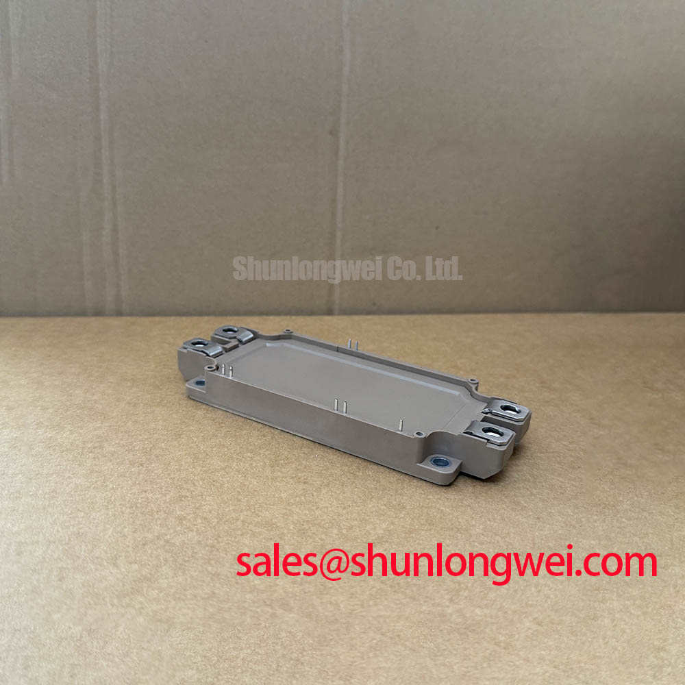
Design Consideration: keep the gate drive loop physically compact and route the gate command with its intended emitter reference return as a close pair. Where the official module connection drawing provides a separate auxiliary emitter or driver-return terminal, use that identified terminal for the driver reference and keep it separate from the main power-emitter path. Do not infer the availability or function of an auxiliary terminal from package appearance alone. Confirm terminal assignment from the applicable Fuji Electric documentation and the original converter schematic before modifying a gate-drive board.
Driver wiring for the upper and lower half-bridge positions should have comparable loop geometry when their switching duties are intended to match. Unequal conductor lengths, different return routing, or a gate board mounted asymmetrically can alter switching behavior even when resistor values are identical. This can appear as unequal voltage overshoot, irregular current waveforms, or intermittent protection events. Oscilloscope probing should reference the correct local emitter point and use a measurement arrangement suitable for fast switching transients; a long probe ground lead can create a misleading waveform.
When investigating nuisance trips, inspect the driver supply at the driver board, the gate-emitter waveform at the module connection, and the collector-emitter waveform under controlled switching conditions. Compare the affected position with the corresponding healthy half-bridge position where safe and applicable. A waveform difference may indicate gate-loop coupling, driver timing variation, busbar asymmetry, or a protection-circuit response. It should not be treated as proof of one specific component failure without measurement.
💡 Pro Tip: Arrange the positive and negative DC bus conductors as a closely coupled, geometrically symmetric path so turn-off overshoot can be evaluated by double-pulse testing against the measured DC-link voltage margin.
Dead-time selection is a system-level Engineering Recommendation, not an attribute of this module. It must prevent cross-conduction while accounting for the installed driver’s propagation behavior, switching transitions, temperature, control architecture, and actual current direction. The freewheel path also deserves measurement because diode reverse-recovery behavior and associated electromagnetic noise depend on operating conditions and the converter layout. The supplied specifications do not establish a reverse-recovery softness factor or a mandatory gate-drive setting for this part.
Assembly Integrity & Layout Architecture: Cosmic-Ray Robustness and Voltage Derating for 2MBI600U4N-120-50
The nameplate boundary to verify first is VCES = 1200 V. During service analysis, record the maximum observed collector-emitter stress at the module terminals rather than relying only on a controller-reported DC-bus value. Cable inductance, laminated-bus geometry, commutation current, protection timing, and measurement location can all change the switching peak seen by the device. The appropriate voltage derating policy is determined by the converter manufacturer’s system requirements and must be validated under representative switching conditions.
Cosmic-ray and neutron-related semiconductor robustness is a high-risk reliability topic. No single-event burnout rate, altitude rating, FIT value, operating-life figure, or immunity claim is stated here for the 2MBI600U4N-120-50. At elevated installation altitude, Design Consideration calls for the equipment owner and system engineer to review applicable manufacturer guidance, site conditions, DC-link stress, insulation coordination, and documented converter qualification requirements. It is not responsible to derive a module-specific single-event failure rate from the voltage rating alone.
The 2500 V AC isolation value is an Official Datasheet Specification for the module. It does not replace the converter-level assessment of creepage, clearance, pollution environment, protective earth arrangement, enclosure condition, and service access. Inspect the mounting area for conductive debris, damaged insulators, displaced busbar supports, and signs that a terminal has moved under mechanical load. Verify that phase connections, DC terminals, and gate-drive terminals follow the official connection diagram before energizing the converter.
Busbars should be supported so their mass and cable forces are not carried by the module terminals. Design Consideration: use a fastening sequence that seats the busbar surfaces evenly and avoids twisting the module during installation. Vibration resistance is governed by the complete assembly, including cabinet support, busbar stiffness, cable restraint, fastener retention method, and maintenance procedure. A visual inspection alone cannot establish long-term mechanical reliability, but it can identify looseness, contact discoloration, displaced supports, and nonparallel mating faces requiring corrective action.
For current-class comparisons within the same voltage family, engineers may review the 2MBI300U4H-120-50 as a reference point. Its presence in an evaluation does not establish electrical, thermal, mechanical, driver, or protection compatibility with the 2MBI600U4N-120-50. Each replacement decision requires a review of the original equipment documentation and measured operating conditions.
2MBI600U4N-120-50 Circuit Protection & Reliability: Calibrating Multi-Module Parallel Current Sharing
Parallel operation begins with equal electrical paths, not with a current probe. The dual half-bridge arrangement of the 2MBI600U4N-120-50 can be used in converter architectures where multiple power positions share load current, but the module rating alone does not guarantee equal sharing among parallel paths. Each branch needs comparable DC-bus impedance, AC-side connection geometry, gate-drive propagation behavior, sensing placement, cooling conditions, and protection response.
At steady state, IGBT conduction characteristics can support thermal balancing under suitable operating conditions because VCE(sat) commonly exhibits a positive temperature coefficient over relevant high-current regions. This is a Design Consideration, not a guaranteed current-sharing specification for this module. Dynamic sharing is often more sensitive to gate-loop layout and commutation-path inductance than static sharing. A branch that switches faster can temporarily carry a disproportionate portion of current even if DC resistance measurements look similar.
Commissioning should therefore compare current and voltage waveforms across intended parallel positions under controlled conditions. Verify that gate commands arrive consistently, that gate-emitter references are local to their respective modules, and that current sensors are interpreted with correct polarity and bandwidth. If one branch shows higher switching stress, investigate busbar geometry, driver supply return paths, sensor placement, timing differences, and cooling asymmetry before changing component values. Protection settings and blanking behavior belong to the complete converter design and should remain aligned with the original equipment protection philosophy.
Thermal symmetry matters as much as electrical symmetry. The specified 0.04 °C/W typical Rth(j-c) describes the junction-to-case path, while the case-to-coolant path can vary substantially with surface flatness, interface application, cold-plate condition, and clamp pressure distribution. Differences between parallel-module temperatures may point to uneven interface contact or coolant flow, but they can also arise from unequal electrical losses. Correlate thermal observations with switching and current measurements before assigning a cause.
Heavy copper busbars dissipate energy through resistive heating, and their temperature rise depends on current, resistance, connection integrity, and heat removal. The physical basis is described in Joule Heating and Thermal Dissipation Modeling in Heavy Copper Busbars. In converter troubleshooting, inspect busbar joints and current-return paths as part of the power-stage assessment rather than treating the IGBT module as an isolated source of heat.
Preventing Spurious Faults: Thermal Interface Material Thickness Uniformity Guidelines for 2MBI600U4N-120-50
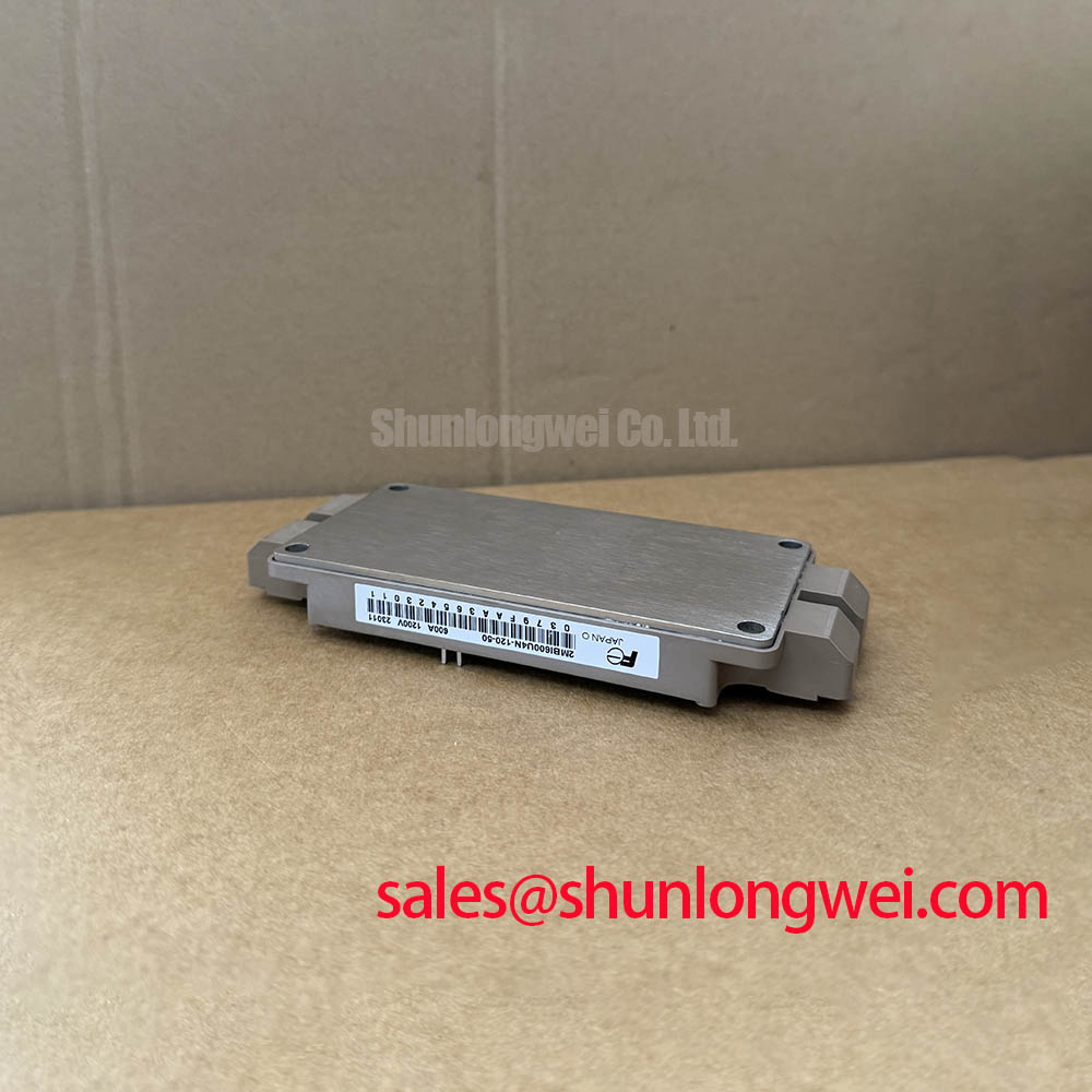
Inspect the cold plate and module baseplate before applying thermal interface material. Remove contamination using a process compatible with the equipment’s maintenance instructions, then assess for scratches, raised debris, corrosion, or distortion that could prevent uniform contact. The 2MBI600U4N-120-50 has a typical 0.04 °C/W junction-to-case thermal resistance, but this value does not include the interface material, cold plate, or coolant circuit. A good internal thermal path cannot compensate for a poorly prepared external contact surface.
Design Consideration: thermal interface material should form a thin, continuous layer that fills surface irregularities without creating excessive separation between the baseplate and cold plate. A general industry application range of 50 to 100 µm is often used as an initial process-control reference for suitable grease-based interfaces, subject to the thermal material supplier’s instructions and the equipment manufacturer’s mounting process. Material type, viscosity, application method, baseplate flatness, and compression behavior determine the correct controlled thickness for the actual assembly.
Apply the module fastening sequence progressively and in a balanced pattern so contact pressure develops across the baseplate rather than concentrating at one corner. The applicable torque, fastener size, washer arrangement, thread condition, and sequence must be taken from the module documentation and converter mechanical drawing. Do not substitute a general torque value for a part-specific mounting requirement. After installation, inspect whether busbar alignment has changed as the module was clamped, since mechanical preload can alter terminal stress and connection coplanarity.
⚠️ Field Alert: Do not tighten power-bus connections or module mounting hardware while stored energy remains on the DC link; isolate, discharge, and verify the equipment safe according to the approved site procedure.
If a converter reports a temperature-related trip after replacement, check coolant circulation, cold-plate contact, interface coverage, mounting sequence, sensor seating, and phase-current balance before attributing the event to the module. An infrared image can help identify uneven external heat patterns, while electrical measurements can determine whether excess switching or conduction loss is contributing. For context on half-bridge behavior and resonant switching analysis, see Resonant Topologies in Home Appliances. Fuji Electric’s Global Power Semiconductor Technologies resource is also relevant when reviewing manufacturer-level power semiconductor information.