



Content last revised on September 29, 2026
Preventing Spurious Faults: Dynamic Power Loss Dissipation and Multi-RC Guidelines for BSM100GB60DLC
| Parameter | Specification |
|---|---|
| Model | BSM100GB60DLC |
| Manufacturer | Infineon |
| Product category | IGBT Module |
| Collector-emitter voltage rating | 600 V |
| Collector current rating | 100 A under the datasheet-specified conditions |
| Package | Module |
Measure the collector to emitter path and gate related terminals with the module isolated, then compare the cold-state readings with a known-good unit before applying the DC link. A diode-test check across the documented antiparallel diode path can reveal an open or abnormal conduction path, but the observed forward reading is test-instrument dependent and should not be treated as a universal pass or fail threshold.
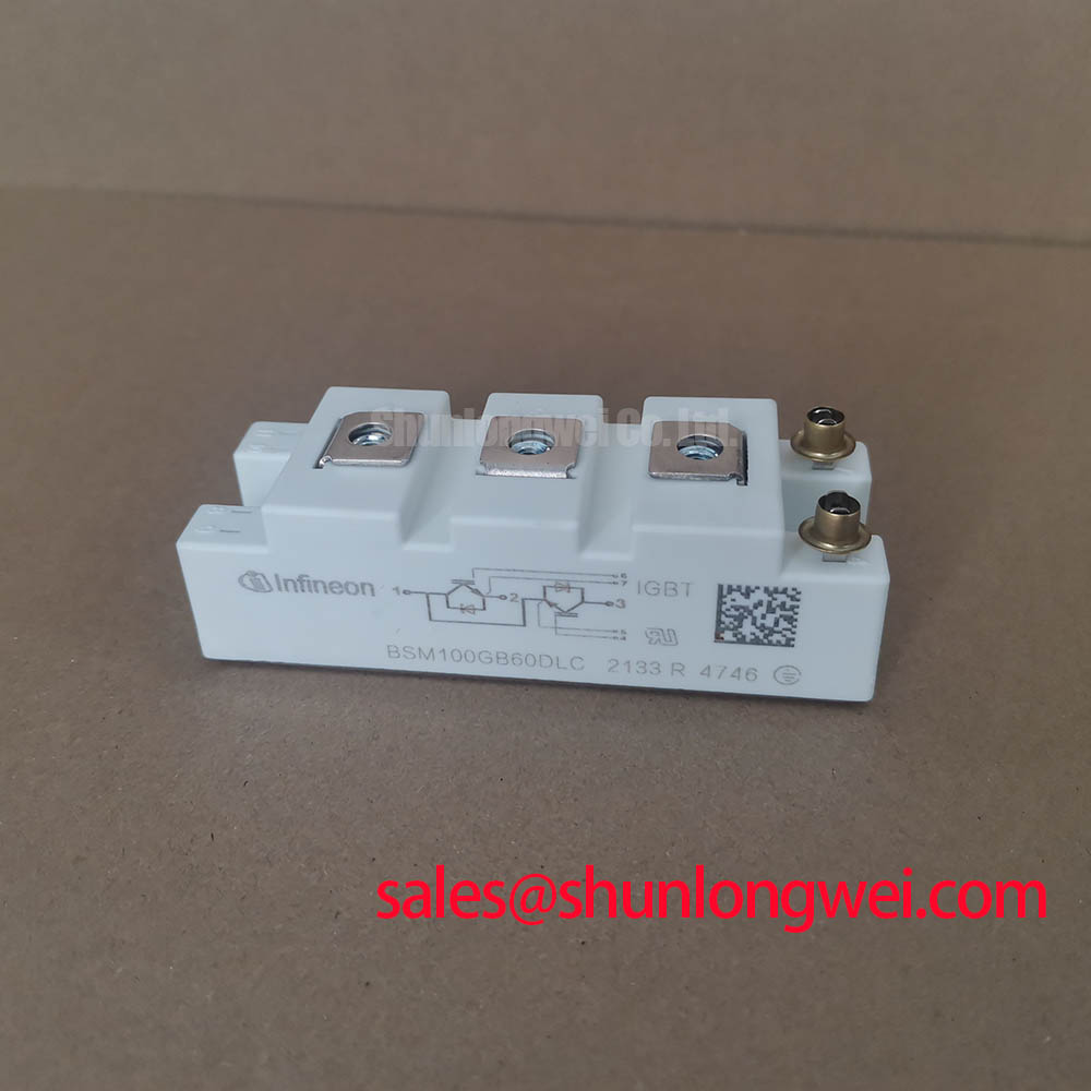
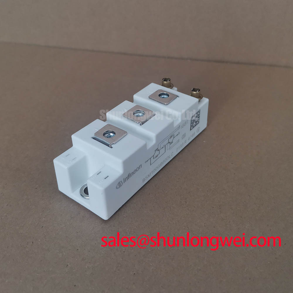
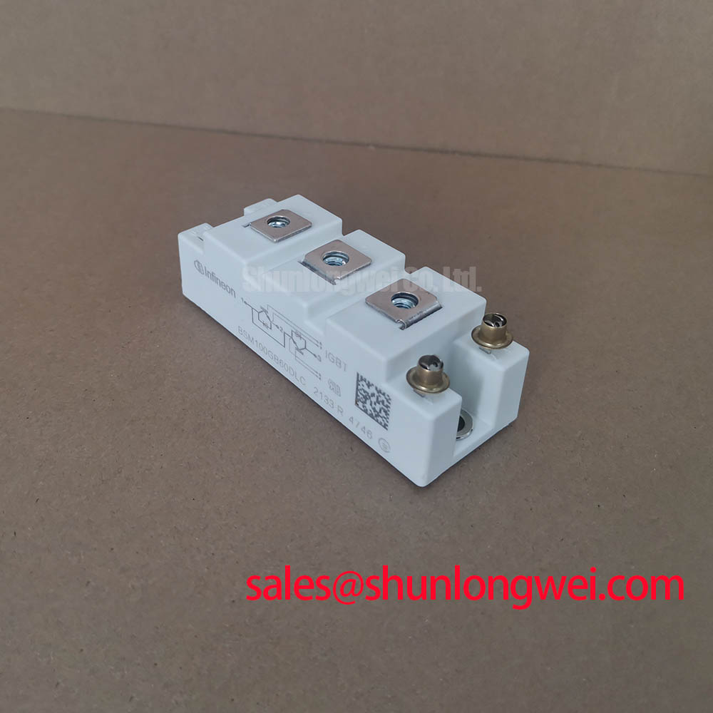
The BSM100GB60DLC is an Infineon IGBT module with a collector-emitter voltage rating of 600 V and a collector current rating of 100 A under the datasheet-specified conditions. These ratings are not a thermal operating guarantee for every switching condition. During incoming inspection, record the part marking, package condition, terminal alignment, and cold electrical baseline. A low-voltage resistance check is useful for detecting gross damage, while insulation verification must use a controlled procedure compatible with the original equipment documentation and the module’s specified limits.
For pulsed overload analysis, treat conduction loss, switching loss, case temperature, and pulse duration as separate contributors. A multi-RC thermal network can translate a measured power pulse into a junction temperature estimate by applying the relevant transient thermal impedances over time. This is an Engineering Calculation, not an Infineon guaranteed field result. The calculation should use validated thermal data for the exact module and heatsink arrangement, then be checked against thermocouple or case-temperature measurements during representative switching tests.
In a utility-scale 1500 V high-power central solar photovoltaic inverter, a 600 V module cannot directly block the full DC-link voltage. Its use would require a topology and voltage-sharing design that keep each device within its ratings. The system designer should also examine bootstrap capacitor recharge behavior where a bootstrap supply is used, diode recovery, gate-driver supply stability, and control-board isolation during repeated switching. The voltage rating of the module does not by itself establish suitability for a particular DC-link topology. Designers should verify voltage overshoot, current pulse duration, cooling performance, and protective coordination at the actual operating point.
Minimize stray inductance in the commutation loop and keep power and control returns separated according to the driver architecture. Clearance and creepage must be selected from the working voltage, pollution environment, insulation system, and applicable equipment standard rather than inferred from the package alone. The Infineon TRENCHSTOP™ IGBT3 application note provides general switching and power semiconductor guidance, but it should not be read as a substitute for model-specific documentation.
Assembly Integrity & Layout Architecture: Mitigating Hard-Switching Transients for BSM100GB60DLC
Capture the gate to emitter waveform and collector to emitter transient with a properly rated differential probe while checking the driver supply at the same instant. A fault that appears only during high-current switching may involve layout inductance, measurement-loop pickup, driver isolation behavior, or protection timing; waveform comparison against a known-good board is more informative than a static continuity check alone.
Short-circuit protection should be evaluated as a complete control function. A sub-10 μs response target and two-stage soft turn-off approach are system-level design choices, not official specifications supplied for this product. The responsible engineer must verify the actual short-circuit withstand capability, detection delay, desaturation behavior, blanking interval, and controlled turn-off profile from the applicable Infineon documentation and qualification data before implementing protection logic.
Hard-switching transients are influenced by busbar geometry, commutation-loop inductance, gate resistance, driver impedance, and the DC-link capacitor connection. Use a compact, symmetrical power path and verify the peak collector-emitter voltage during turn-off. The design objective is to suppress inductive overshoot while maintaining sufficient switching speed, with final margins established through oscilloscope testing at the worst credible current, temperature, and supply conditions.
When modules are operated in parallel, static current sharing should be assessed rather than assumed. Device parameter spread, thermal coupling, emitter connection resistance, gate-loop mismatch, and busbar symmetry all affect the result. A positive temperature coefficient of on-state voltage can support balancing under some operating conditions, but it does not eliminate dynamic sharing errors. Confirm current distribution with matched measurement points and representative thermal cycling.
For an inverter service replacement, the BSM100GAL120DN2 should be treated only as a separate candidate for engineering comparison. Voltage class, current rating, switching behavior, package, pin arrangement, thermal interface, and protection requirements must be matched against the original design before any substitution is considered.
BSM100GB60DLC Circuit Protection & Reliability: Calibrating Dynamic Gate Impedance Control
Check the gate-emitter impedance, driver output at the module terminals, and the isolation barrier response before attributing unexpected turn-on to the IGBT itself. Compare the command waveform with the gate waveform under common-mode transients; a difference between the two can indicate driver-loop coupling, insufficient isolation performance, or an unintended return-current path.
High dv/dt operation requires a coordinated gate-drive layout. A dedicated active Miller clamp may be evaluated where the driver architecture supports it, but its use is an Engineering Recommendation that depends on the confirmed terminal configuration and switching conditions. Negative gate bias, including values sometimes used in industrial gate-drive designs, must not be applied without verification against the exact gate-emitter rating and driver documentation for this module.
Where a bootstrap supply is used, it deserves a separate bench check. Measure capacitor voltage during the complete high-side switching sequence, inspect recharge time, and observe diode recovery current at the driver board. The required capacitance, recharge margin, and diode selection are determined by gate charge, switching frequency, duty cycle, isolation arrangement, and driver losses. These values cannot be inferred from the 600 V and 100 A product ratings.
Industrial drive boards using optocouplers or digital isolators should be tested for common-mode transient immunity under the installed mechanical layout. Confirm isolation-barrier voltage behavior, propagation delay, power-supply decoupling, and fault-state response. The module does not independently provide system-level EMC compliance; the completed inverter must be evaluated as an assembly under the applicable requirements.
Where the package provides separate auxiliary emitter or control terminals, route those connections independently from the high-current emitter path and verify the terminal definition from the original mechanical drawing. Do not assume a Kelvin function or assign an auxiliary terminal without documentation. A clean reference at the driver pins is especially important when two-stage turn-off or active clamping is used.
Benchtop Waveform Tuning: Voltage Derating and Cosmic-Ray Reliability Considerations for BSM100GB60DLC
Use a differential high-voltage probe to record the collector-emitter peak during turn-off, then repeat the measurement across load current, temperature, and DC-link conditions. Compare the measured peak with the documented voltage boundary and investigate ringing frequency, damping, probe placement, and switching-loop geometry before changing the gate-drive setting.
Cosmic-ray effects, terrestrial neutron exposure, single-event burnout, FIT rate, altitude derating, and lifetime prediction require authoritative device-specific reliability data. No such data is supplied in the stated product parameters, so a numerical SEB probability or operating-life estimate cannot be assigned to the BSM100GB60DLC from those parameters alone. Treat these subjects as a Design Consideration and obtain the relevant qualification evidence when the equipment operates at elevated altitude or in applications with demanding continuous availability.
Voltage derating should be established from the actual DC-link waveform, switching overshoot, environmental conditions, insulation coordination, and the manufacturer’s reliability guidance. A 1500 V photovoltaic inverter topology cannot be judged from the nominal solar-array voltage alone; the voltage across each 600 V device must remain within its specified limits. The system engineer should verify peak margins during switching tests, including abnormal control states, regeneration, grid disturbances, and fault interruption.
Where phase-controlled rectifier sections are present, they can introduce line-current distortion and high-frequency interaction with the inverter DC link. Evaluate conduction angle, DC-link ripple, harmonic filtering, and control-loop interaction at the equipment level. The module rating does not certify compliance with grid harmonic or EMC requirements, and the completed photovoltaic power-conversion system must be assessed against its applicable grid code and installation standard.
For broader application context, the Industrial Applications guide can be used alongside the original device documentation when reviewing renewable-energy and heavy-industry topologies.
💡 Bench Tip: Use ESD protection and discharge the DC link fully before disconnecting the gate-driver cable or comparing cold-state terminal measurements.