
Content last revised on September 10, 2026
BSM10GP120 Repair and Application Considerations
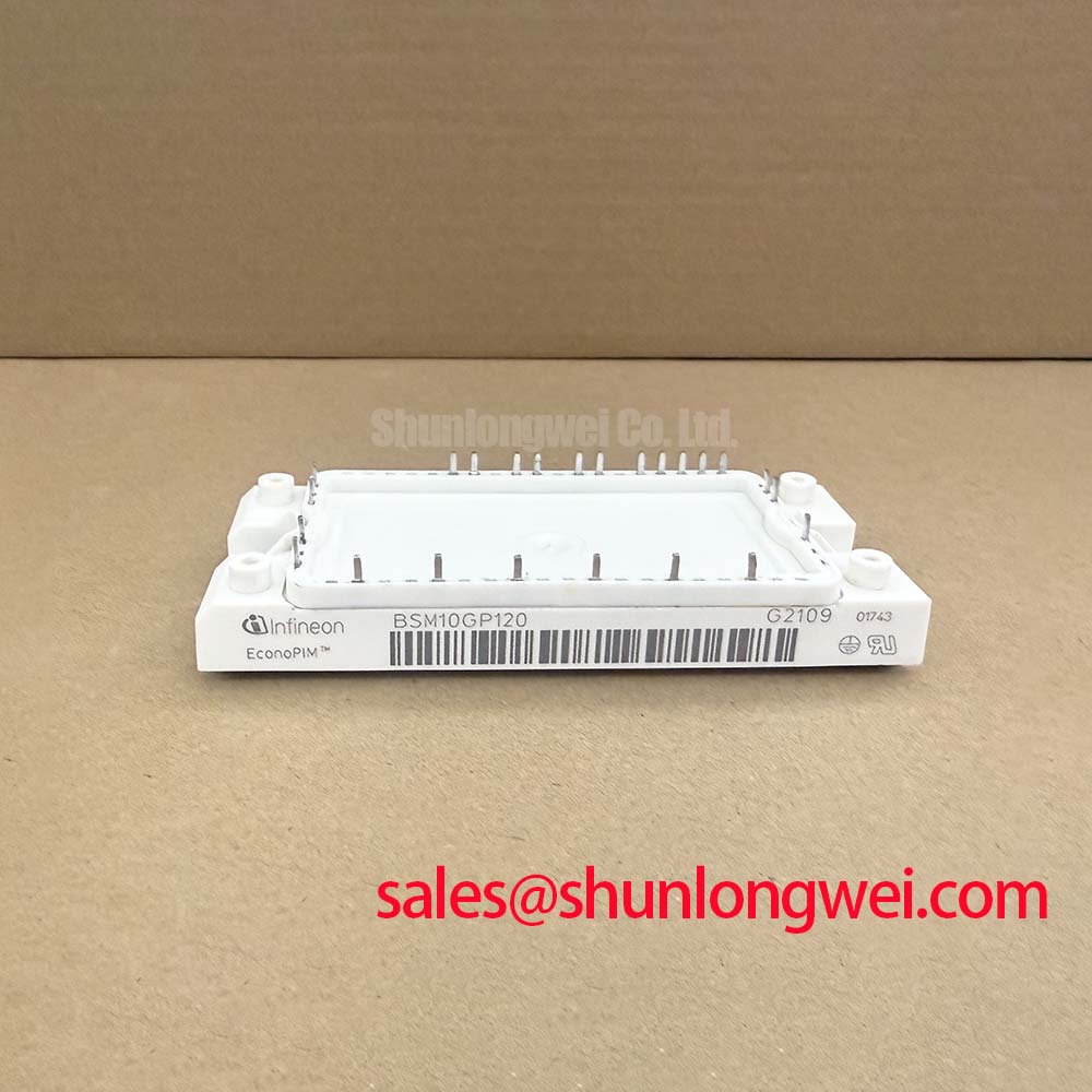
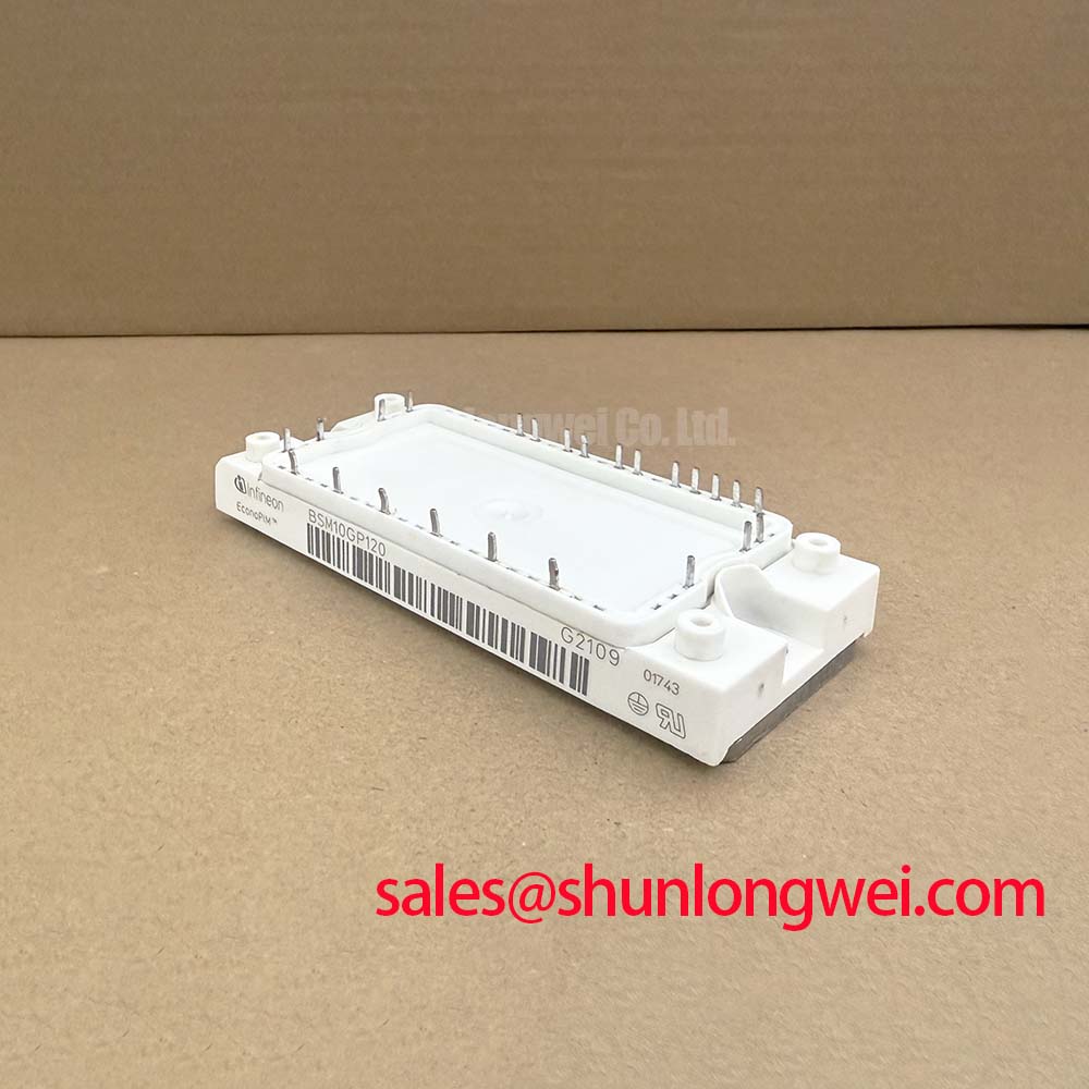
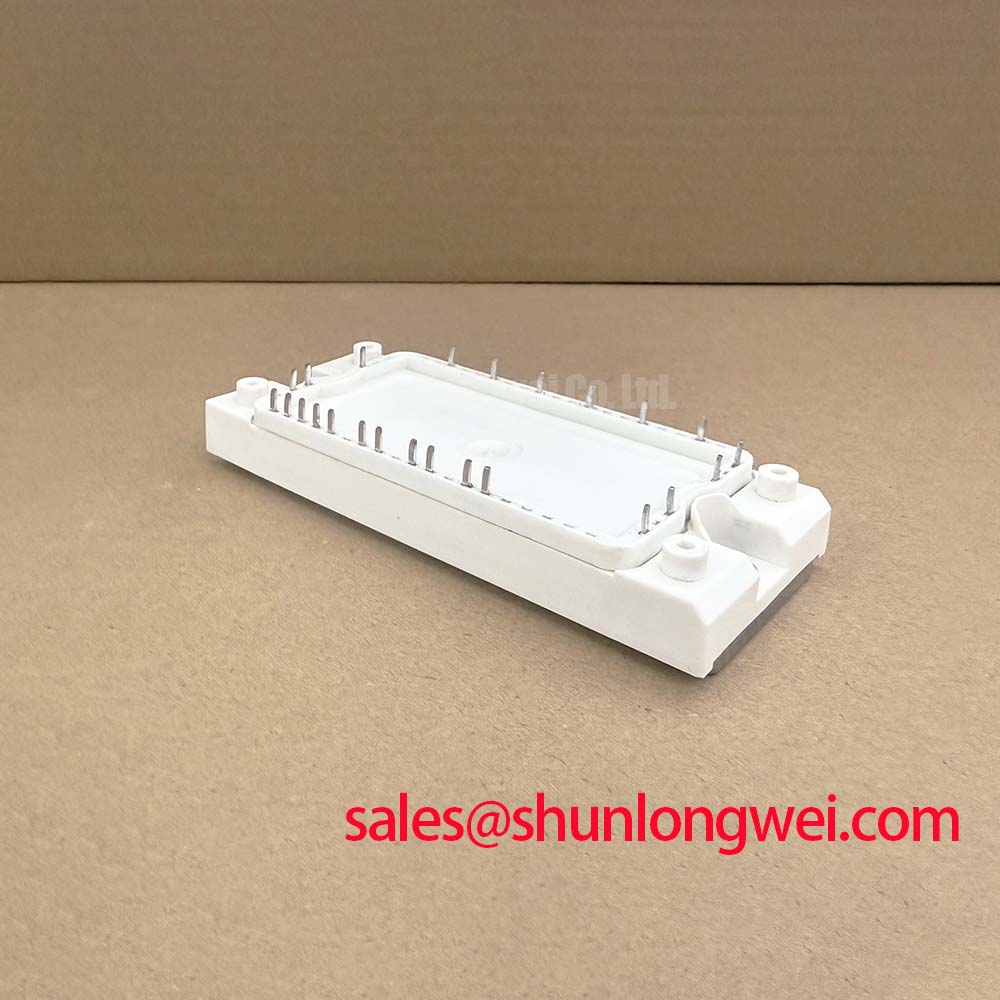
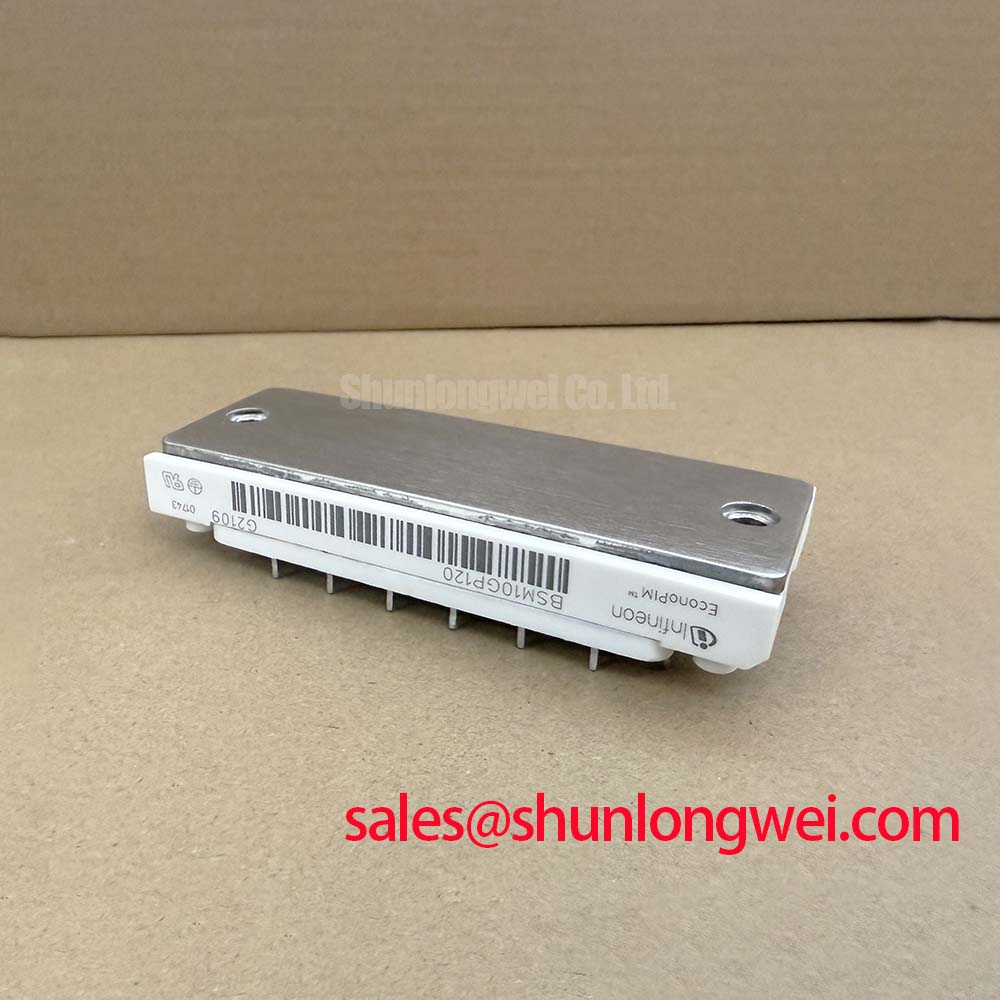
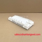
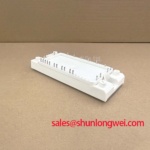
Verify the nameplate rating, power terminals, control terminals, housing condition, and cold-state isolation from the surrounding assembly before fitting the BSM10GP120 into a repaired drive. This Infineon IGBT module is rated at 1200 V and 10 A as an Official Datasheet Specification, with a Module housing. These ratings establish the device identity and must be checked against the original inverter schematic, DC link voltage, motor load profile, gate driver arrangement, and cooling assembly before commissioning.
For repair and sourcing work, the module should be evaluated as part of its original switching position rather than as an isolated current rating. A compact industrial inverter or high speed CNC spindle drive can impose repetitive switching stress, cable reflected voltage, and temperature cycling conditions that depend on the complete system. The system integrator should verify all application specific electrical limits from the original equipment documentation and the applicable Infineon product documentation.
| Manufacturer | Infineon |
| Product model | BSM10GP120 |
| Collector emitter voltage rating | 1200 V Official Datasheet Specification |
| Rated current | 10 A Official Datasheet Specification |
| Housing format | Module Official Datasheet Specification |
Assembly Integrity and Layout Architecture for BSM10GP120
Start thermal assembly by removing aged interface residue from both the module mounting face and heatsink contact surface without scratching either surface. Inspect the heatsink for flatness, debris, corrosion, and local damage around mounting points. A thermal interface layer that is too thick, uneven, or interrupted by trapped air can raise thermal resistance and make a normal electrical load appear to be a semiconductor fault. Thermal paste thickness control within the general industry range of 50 to 100 μm is a Design Consideration, not an Infineon factory specification for this module.
Apply the interface material as a thin, continuous layer suitable for the selected compound and mounting surfaces. The purpose is to fill microscopic surface irregularities rather than create a thick insulating layer. If the baseplate and heatsink surfaces do not mate evenly, the mounting process should compensate through controlled fastening sequence and inspection rather than excessive paste application. Uneven pressure can leave portions of the module inadequately coupled to the heatsink, particularly after service work where the mechanical stack may have been disturbed.
Fasten mounting hardware in a progressive cross pattern so pressure spreads across the mounting area gradually. The correct torque, screw specification, washer arrangement, and tightening sequence must be verified from the module mechanical documentation and the original equipment assembly drawing. This is particularly important when a replacement module is fitted into an existing inverter frame whose heatsink or hardware may differ from the initial production assembly.
💡 Pro Tip: Keep the DC link bus path physically compact and symmetrical around the switching loop, then verify turn off peak voltage with switching tests under the actual system conditions.
Layout work should separate the high current power path from gate control conductors wherever practical. Parasitic inductance in the collector, emitter, capacitor, and busbar loop contributes to voltage overshoot during switching. This is a Design Consideration: minimize loop area to suppress inductive overshoot, while the system engineer validates peak voltage against the DC link voltage and the module’s 1200 V rating during controlled testing.
Where a repair requires comparison against another component in a related voltage and current class, FP10R12KE3 can be reviewed as a separate reference model. Electrical ratings alone do not establish drop in compatibility. Terminal arrangement, internal circuit configuration, driver interface, thermal contact geometry, and protection behavior must be confirmed from documentation before any substitution decision.
Field Diagnostics and Commissioning for Dual Switch BSM10GP120 Circuits
Before power is applied, verify that the gate driver outputs correspond to the correct module control terminals and that the inverter control logic prevents unintended simultaneous conduction in the switching leg. Check the DC link capacitor connections, busbar fastening, motor output connections, and driver supply references. A damaged gate resistor, shifted driver reference, poor control connector contact, or incorrect gate sequence can each produce abnormal switching behavior, so diagnostic work should isolate each possibility through measured evidence.
In dual switch topologies, the main high current emitter path and the driver return path need careful treatment. Shared emitter inductance can couple load current transients into the gate loop, altering the effective gate voltage during a switching transition. As a Design Consideration, route the driver return through the intended low inductance reference path identified by the module and gate driver documentation, rather than allowing it to share a long high current emitter route. Oscilloscope measurements should use a probing method appropriate for floating power circuits and should compare gate emitter voltage with collector emitter switching behavior.
Gate loop wiring should remain short, direct, and consistent between corresponding devices in a bridge arrangement. If one device has a materially different physical path, its switching transition may differ from the opposite device even when the control command is identical. Engineers should inspect gate resistor placement, connector seating, return routing, and driver board grounding before changing component values. Changing damping components without observing the actual switching waveform can conceal rather than resolve a layout issue.
Short circuit protection is determined by the complete driver and controller design, not by the BSM10GP120 ratings listed here. Desaturation sensing based on collector emitter voltage is commonly used in IGBT driver circuits as a Design Consideration. The protection timing, blanking interval, fault threshold, and soft turn off behavior must be set and verified against the particular driver documentation, switching topology, and fault energy capability. A controlled two stage turn off response can reduce the risk of a severe transient, but it must be validated at system level rather than assumed from the module designation.
For driver architecture context, the Infineon EiceDRIVER™ galvanic isolated gate driver IC portfolio provides relevant technical categories for isolated control and protection implementation. The final driver choice and its commissioning settings remain system determined.
Thermal Feedback and Current Balance in BSM10GP120 Switching Positions
After initial low energy commissioning, thermal behavior should be evaluated while the system operates through its intended load conditions. Measure heatsink temperature at repeatable locations, monitor controller fault records, and inspect switching waveforms when practical. A rise in temperature can result from reduced heatsink airflow, degraded interface material, restricted cabinet ventilation, unexpected load duty, gate drive instability, or imbalance elsewhere in the converter. No single observation should be treated as proof of one root cause.
For IGBT devices operating in parallel arrangements, static current sharing is influenced by the temperature dependence of collector emitter saturation voltage. This is a Design Consideration, not a guarantee of equal current division in every layout. Dynamic sharing during switching is also affected by gate loop impedance, busbar symmetry, controller timing, and the physical placement of DC link capacitors. When parallel paths exist, engineers should compare equivalent paths rather than assume that equal component labels produce equal switching stress.
The 10 A current rating is an Official Datasheet Specification for the module, but equipment load current and semiconductor junction conditions are not interchangeable values. A spindle drive can experience load changes during acceleration, deceleration, cutting operations, or control events. The system designer should establish operating margin using the original application requirements, measured thermal performance, switching loss behavior, cooling capability, and the manufacturer’s complete datasheet limits.
At service level, inspect for signs that the thermal stack has shifted after repair, including loose mounting hardware, displaced insulation parts, blocked airflow paths, or a heatsink surface contaminated by old compound. Repeat measurements under comparable load conditions after corrective work. This approach provides evidence of whether thermal behavior changed with the mechanical repair instead of attributing the outcome solely to the power module.
The Infineon IGBT modules and discretes portfolio is a useful authority reference for understanding the broader device category. For equipment level evaluation, the exact BSM10GP120 documentation and original drive design remain the controlling sources.
Transmission Line Impedance Checks for BSM10GP120 Motor Outputs
Long motor cables can behave as transmission lines during fast inverter switching events. An impedance discontinuity between inverter output, cable, and motor terminals can create reflected voltage waves. Depending on cable length, motor characteristics, switching conditions, grounding arrangement, and termination behavior, the motor terminal waveform can differ substantially from the inverter output waveform. Engineers should measure at relevant locations with suitable high voltage differential probing rather than infer motor terminal stress solely from a measurement at the module bus.
When commissioning a compact industrial inverter or high speed CNC spindle drive, inspect the motor cable for routing changes, damaged shielding, loose terminals, unsuitable extensions, and unexpected joints. These conditions may contribute to waveform distortion, common mode noise, or reflected peaks. If abnormal voltage behavior is observed, evaluate whether output reactors, dv dt filters, sine filters, cable specification, and motor insulation requirements are appropriate for the full drive system. Filter selection is a system level Engineering Recommendation and must be verified under actual cable and motor conditions.
The module layout also matters because inverter output noise can couple back into the gate driver and control electronics. Maintain clear separation between switching nodes and sensitive signal wiring, use the grounding strategy defined by the equipment architecture, and confirm that protection signals remain stable during motor operation. A fault that appears only after the motor cable is connected may indicate interaction among cable impedance, output filtering, grounding, driver immunity, and switching loop layout. Waveform capture across known operating states is more reliable than replacing parts based on symptoms alone.
For engineers evaluating power semiconductor technology choices and switching behavior at a broader level, this Wide Bandgap Revolution resource provides additional design context. Any transition from an IGBT module to a different semiconductor technology requires a complete review of topology, driver behavior, thermal design, protection coordination, and EMC performance at equipment level.
Where the same equipment contains related power stages, BSM75GD120DLC is a separate module reference for topology review. Its presence in a design comparison does not establish electrical or mechanical interchangeability with the BSM10GP120.