

Content last revised on September 26, 2026
FZ1000R33HL3 Transient Dynamics and Electrical Design
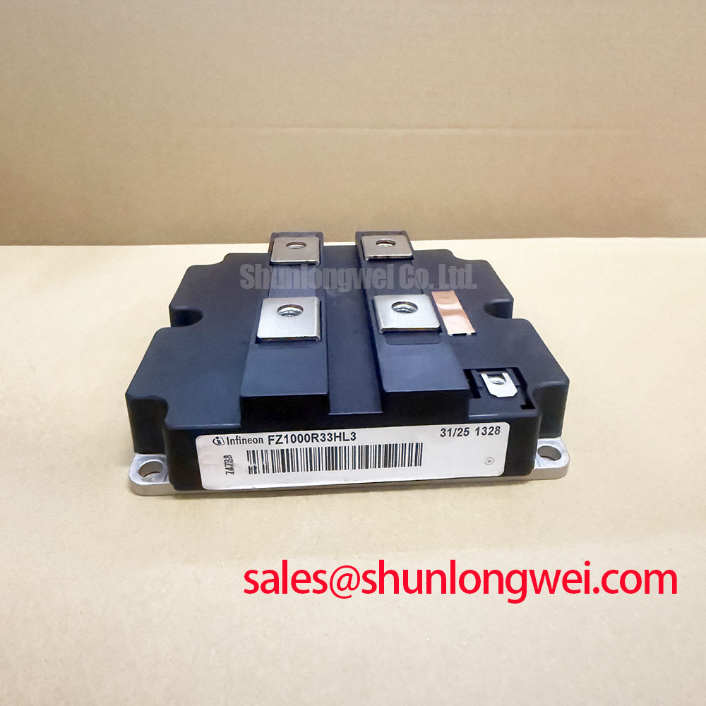
With the DC link isolated and discharged, check the installed module’s identification and record cold-state terminal measurements before assessing FZ1000R33HL3 for a repair. Infineon specifies a 3300 V voltage rating and 1000 A current rating for this IGBT module (Official Specification). Those ratings establish component boundaries; they do not, by themselves, establish compatibility with an existing gate driver, busbar, cooling assembly or protection circuit.
A utility-scale 1500 V central solar photovoltaic inverter is one possible system in which an engineer might evaluate this module. The relevant comparison is not simply DC-link voltage against the module’s voltage rating. During turn-off, stray inductance can raise the collector-emitter peak above the steady DC-link level. As a Design Consideration, keep the commutation path compact and examine measured peak voltage under the inverter’s actual switching conditions. The system engineer must determine the allowable operating margin using the applicable Infineon documentation, the assembled inverter and its test results.
Before substituting a module, compare its documented terminal arrangement, mounting interface, cooling requirements and gate-drive conditions with the equipment drawings. FZ3600R12HP4 can be included in a parameter comparison, but its different voltage and current ratings mean it should not be treated as a direct replacement on the basis of product family or manufacturer alone. In the wider power-conversion chain, FZ800R12KS4_B2 is another module an engineer may encounter when reviewing associated converter stages; its circuit role and suitability require a separate schematic-level check.
Altitude, terrestrial radiation and single-event burnout warrant system-level attention where the installation demands it, but the supplied ratings do not support a numerical FIT estimate, an altitude derating curve or a guaranteed safe DC-bus threshold for this model. As a Design Consideration, request the manufacturer’s applicable reliability guidance before assigning such limits. For broader application context, Industrial Applications provides a starting point for reviewing operating conditions; it does not replace module-specific qualification data. During fault investigation, retain the DC-link, gate and collector-emitter waveforms so an apparent voltage-margin problem can be distinguished from a measurement or control-sequence problem.
FZ1000R33HL3 Thermal-Electrical Optimization: Current Sharing and Gate Timing
The 1000 A current rating (Official Specification) is a module rating, not permission to assume equal current in parallel positions or adequate capacity under every cooling condition. When multiple modules share a current path, compare their physical connections and measured operating behaviour before changing the gate circuit. Differences in busbar impedance, gate-loop routing, thermal contact and device characteristics can affect sharing. Whether a positive temperature coefficient of on-state voltage assists static sharing at a particular operating point must be established from the relevant characteristic curves rather than assumed across the full load range.
Dynamic sharing needs its own check. A symmetric power path and closely matched gate-loop routing are Design Considerations intended to reduce differences during switching. Measure the gate-emitter and collector-emitter waveforms at comparable locations for each position, using appropriate high-voltage measurement practices. If one position switches noticeably earlier, inspect drive timing, connection resistance and loop geometry before attributing the difference to the module. Infineon’s IGBT paralleling application note discusses the mechanisms that make static and dynamic balance separate engineering tasks.
Complementary switching adds a timing constraint: the outgoing device must cease conducting before the opposing device is allowed to turn on. Dead time that is too short can permit cross-conduction; excessive dead time can alter current paths and switching behaviour. No fixed dead-time value follows from the voltage and current ratings alone. As a Design Consideration, verify the driver interlock, propagation delays and gate waveforms over the intended operating conditions, then set timing from the tested system response. Keep the interlock’s control connections and each gate return path identifiable in the wiring documentation so a repair does not inadvertently change the validated arrangement.
Desaturation protection also requires circuit-level verification. An elevated collector-emitter voltage while the device is commanded on can be consistent with an overcurrent event, but the recorded gate command, current and voltage traces are needed to interpret it. Check that the driver detects the condition and performs its intended soft turn-off without producing an unacceptable voltage overshoot. Short-circuit safe operating area cannot be inferred from the 3300 V and 1000 A ratings; use the applicable manufacturer limits and the inverter’s protection test procedure before accepting the setup.
FZ1000R33HL3 Junction-to-Case Thermal Response and Mounting Checks
For a pulsed-load assessment, start with the inverter’s measured current, switching pattern and case-temperature history. Junction temperature responds to both the size and duration of dissipated power, so a steady-state thermal estimate can miss the peak reached during a short overload. An Engineering Calculation can use the manufacturer’s junction-to-case transient thermal-impedance data with the relevant power-loss waveform to estimate that peak. The information supplied here does not include a transient thermal-impedance curve, loss tables or a maximum junction-temperature value; a defensible numerical peak-temperature margin therefore requires the applicable Infineon datasheet and system measurements.
Keep the thermal boundaries distinct in that calculation. Junction-to-case response describes the module-side transient behaviour, while the interface to the heatsink and the heatsink’s response depend on the assembly. A multi-RC representation may be useful for a time-domain simulation if its parameters come from the correct module documentation. It should not be populated with assumed values merely because the resulting temperature trace appears plausible. Compare the simulation against measured case and heatsink temperatures at repeatable load points, allowing for sensor location and thermal lag.
On the bench, inspect the mounting surface for damage or contamination and check that the module seats consistently against the heatsink. Apply the specified thermal-interface material and follow the applicable mounting instructions for coating method and fastener sequence. Neither a grease thickness nor a bolt torque has been established by the supplied product data, so those values must come from the approved module and mechanical assembly documentation rather than a generic shop setting. If temperatures differ between otherwise comparable positions, examine contact quality, coolant flow, sensor placement and electrical loss before assigning a single cause.
Intermittent thermal alarms deserve the same record-based approach. Capture load, case temperature, heatsink temperature and the protection event together; an alarm that appears during a current pulse does not prove the junction crossed its limit. Likewise, a cool external surface immediately after a brief event does not rule out a higher transient junction temperature. The practical objective is to connect the observed event to a documented thermal model and the actual assembly, then decide whether further instrumented testing is necessary.
FZ1000R33HL3 Active Miller Clamp and Spurious Turn-On Checks
During rapid switching of a complementary device, changing collector-emitter voltage can couple through an IGBT’s internal capacitance and disturb its gate voltage. An active Miller clamp is a driver-level method of holding the off-state gate near its intended reference when the driver and layout support it. For FZ1000R33HL3, the supplied specification does not establish a gate-drive voltage, a required negative bias or a prescribed clamp circuit. Those choices belong to the validated driver design and the applicable manufacturer guidance, not to the module’s headline ratings.
As a Design Consideration, place the clamp’s return path so it does not add a long shared impedance to the gate loop. Check gate-emitter voltage at the module connection during the fastest relevant opposing-device transitions and during protection turn-off. A visible gate excursion calls for investigation, but it does not alone prove cross-conduction: compare it with the driver command, collector-emitter waveform and current measurement. Infineon’s official IGBT portfolio is a manufacturer reference for locating the appropriate product documentation before changing a gate-drive design.
Pro Tip: Keep paired busbar and gate-return paths as symmetric as the assembly permits, then verify turn-off overshoot and off-state gate behaviour with switching tests before accepting the layout. If a repaired inverter develops intermittent gate or desaturation faults, first compare its present wiring and driver configuration with the documented installation. Record waveforms before adjusting clamp behaviour, dead time or protection thresholds; each change can affect a different part of the same switching event.