

Content last revised on September 26, 2026
Field Diagnostics & Commissioning: Static and Dynamic Current Distribution in FZ1200R33KF2C_B3_S2 Topologies
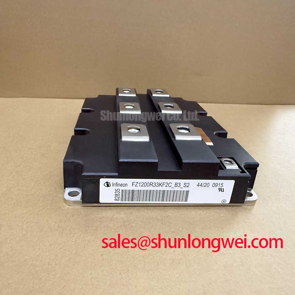
Before energizing a replacement, isolate the traction inverter, inspect the power terminals and baseplate, then verify the nameplate boundary against 3300 V VCES and 1200 A continuous DC collector current. For a cold bench check, compare terminal impedance and diode-like junction behavior with a known-good unit while avoiding insulation tester voltages that exceed the approved service procedure.
| Parameter | Official specification | Engineering significance |
|---|---|---|
| Collector emitter voltage | 3300 V | High voltage blocking for industrial and traction converter DC links |
| Continuous DC collector current | 1200 A | Supports high power switching when thermal and electrical conditions are verified |
| Isolation test voltage | 10.2 kV AC for 1 minute | Relevant to module insulation verification; not a field test instruction |
| Collector emitter saturation voltage | Typical 3.45 V at 1200 A and Tj = 125°C | Important for conduction loss assessment and cooling review |
| Baseplate | AlSiC | Provides a ceramic compatible thermal expansion interface |
| Package | IHM B, 190 mm | Defines the mechanical envelope and mounting compatibility check |
These values are official product parameters supplied for this device. They are not a substitute for the complete Infineon documentation covering gate limits, switching energy, short circuit capability, terminal arrangement, thermal impedance, and mechanical fastening requirements. The Infineon PrimePACK™ reference is useful when checking the wider module family and application context. A system integrator evaluating a high speed rail or heavy freight locomotive traction inverter should confirm the exact mechanical drawing and electrical interface before approving a field replacement.
Start with a de energized inspection of the collector and emitter bus connections, ceramic isolation areas, baseplate flatness, and signs of localized thermal discoloration. A cold resistance comparison can identify an obvious short circuit or an abnormal open connection, but it cannot prove switching health. For that decision, compare gate to emitter behavior, driver supply integrity, command timing, and collector emitter waveforms with a serviceable phase leg.
For parallel IGBT paths, static current sharing is influenced by the positive temperature coefficient associated with the saturation voltage in the relevant operating region. That characteristic can support balancing, but only when semiconductor matching, thermal coupling, busbar symmetry, and gate drive conditions are also controlled. Treat this as a Design Consideration, not as a guaranteed sharing result for every converter topology. Equal length gate wiring, similar power path impedance, and matched thermal mounting should be verified during commissioning.
Dynamic imbalance often appears only during turn on and turn off. Use isolated differential probes and current measurement equipment rated for the inverter environment, then compare collector emitter overshoot, turn off slope, ringing, and gate voltage at each device. If one path shows a different waveform, inspect the complete gate loop and power commutation path rather than assigning the fault to the module alone. The required clearance and creepage distances are system determined by working voltage, pollution environment, insulation system, and applicable standards. Engineers should validate them against the original traction inverter design and the relevant safety file.
De saturation protection can provide a controlled response to an overcurrent event when the driver has a verified detection threshold, blanking interval, soft turn off function, and fault latch. The module data listed here does not establish a specific de saturation threshold or short circuit safe operating area. Designers should obtain those limits from the applicable Infineon documentation and confirm the complete protection sequence on a controlled test fixture. A replacement evaluation may also be compared with the neutral reference device FZ3600R12HP4 when the equipment documentation identifies it as a valid comparison, but electrical and mechanical interchangeability must be proven by the system engineer.
Preventing Spurious Faults: Thermal Interface Control and Mounting for FZ1200R33KF2C_B3_S2
The AlSiC baseplate must sit against a clean, stable heatsink surface. Remove old interface material without scoring the mating area, inspect for burrs, and confirm that the mounting surface does not force the module into local distortion. A thin, continuous thermal interface layer is generally preferred; a typical engineering starting range of 50 to 100 µm may be considered only when it matches the compound supplier’s application data and the measured surface condition. The final thermal result should be verified through temperature measurement under the intended load.
Void control is a practical service issue. Excess compound can increase thermal resistance and contaminate adjacent insulation surfaces, while insufficient compound can leave dry regions beneath the baseplate. Apply the material consistently, lower the module without sliding it across the heatsink, and tighten the fasteners in a staged diagonal sequence. The correct torque is determined by the fastener, washer, thread condition, module drawing, and heatsink design, so the original assembly instruction takes priority over a generic value.
Thermal paste degradation may present as rising case temperature, uneven phase temperatures, or repeated protection trips, but those symptoms require measurement rather than a single assumed cause. Check cooling flow, sensor placement, busbar loading, switching frequency, and gate timing before removing the module. A thermal imaging survey can help locate imbalance, provided the optical surface and measurement method are suitable for the inspection.
Fast semiconductor fuse coordination is another commissioning checkpoint. The fuse clearing I2t must be evaluated against the converter fault current, wiring inductance, protection delay, and the device’s documented surge and short circuit limits. The module’s 1200 A continuous rating alone cannot establish fuse suitability. Verify the complete clearing sequence during a controlled fault study and confirm that the fuse does not allow energy beyond the approved device capability.
Field Alert: Never loosen or insert module power and gate connections while the DC link, auxiliary supply, or stored energy circuit remains connected.
Assembly Integrity & Layout Architecture: Galvanic Gate Drive Isolation for FZ1200R33KF2C_B3_S2
The stated 10.2 kV AC isolation test voltage for 1 minute is an important module insulation specification, but it does not automatically certify the complete gate driver, transformer, connector, PCB, or traction inverter assembly. The gate drive barrier must be assessed as a system. Designers should verify reinforced isolation, creepage, clearance, insulation materials, common mode transient performance, and the applicable railway or industrial compliance requirements using the driver manufacturer’s data and the equipment safety analysis.
Do not transfer thyristor gate values such as IGT and VGT to this component. This is an IGBT module, so its gate charge, gate voltage limits, turn on and turn off behavior, short circuit response, and driver supply requirements must come from the applicable IGBT documentation. A strong pulse or pulse train may be appropriate in some thyristor circuits, but it is not a valid substitute for an IGBT gate drive design review.
When diagnosing nuisance faults, monitor the gate emitter waveform at the module terminals rather than only at the driver output. Look for common mode displacement, insufficient isolation barrier behavior, unequal propagation delay, ground reference movement, and coupling from the collector power loop. If a driver is specified with a high CMTI capability, confirm that the installed PCB layout, isolation component, supply decoupling, and probe arrangement preserve that performance. Avoid presenting any unverified CMTI figure as an FZ1200R33KF2C_B3_S2 product rating.
Benchtop Waveform Tuning: PCB Gate Loop Symmetry and Switching Stress
Waveform tuning should begin at reduced energy with the DC link, load, gate resistance, and protection settings selected according to the approved test plan. Keep the gate drive path compact and symmetrical, separate high di/dt collector current paths from sensitive gate signals, and return the gate drive reference through the terminal arrangement confirmed by the module drawing. Do not assume a Kelvin emitter connection unless it is explicitly identified for this exact module.
Mutual coupling between the power emitter path and the gate return can create ringing, false turn on, or excessive gate voltage excursion. A practical investigation compares the gate emitter waveform at the module, the driver output waveform, and the collector emitter transition on the same time base. If the gate signal changes when the main power path is switched, inspect layout coupling, connector pin assignment, isolated supply impedance, and probe loop area before changing the gate resistor.
Soft turn off during de saturation protection can reduce the electrical stress created by a rapid interruption of fault current, but its timing and slope are system functions. The driver must be checked against the module’s documented short circuit operating limits, desaturation response requirements, and safe operating area. Dead time should prevent complementary devices from conducting simultaneously, while the actual value remains dependent on propagation delay, temperature, driver mismatch, and switching test results.
For high voltage traction converter work, the switching test should record DC link voltage, collector emitter voltage, gate emitter voltage, phase current, and protection timing. Minimize parasitic commutation inductance to control turn off overshoot, then verify peak voltage margins against the 3300 V blocking rating during real switching conditions. The application discussion in Wide Bandgap Revolution can provide wider context for fast switching design choices, while the Infineon TRENCHSTOP™ IGBT3 application note offers additional manufacturer technical context. The final acceptance decision should be based on measured waveforms, verified insulation, thermal performance, and the original equipment manufacturer’s interface requirements.