Content last revised on October 21, 2026
Field Diagnostics & Commissioning: Preventing Internal Leadframe Cracking in FZ1200R33KF2-B5 Topologies
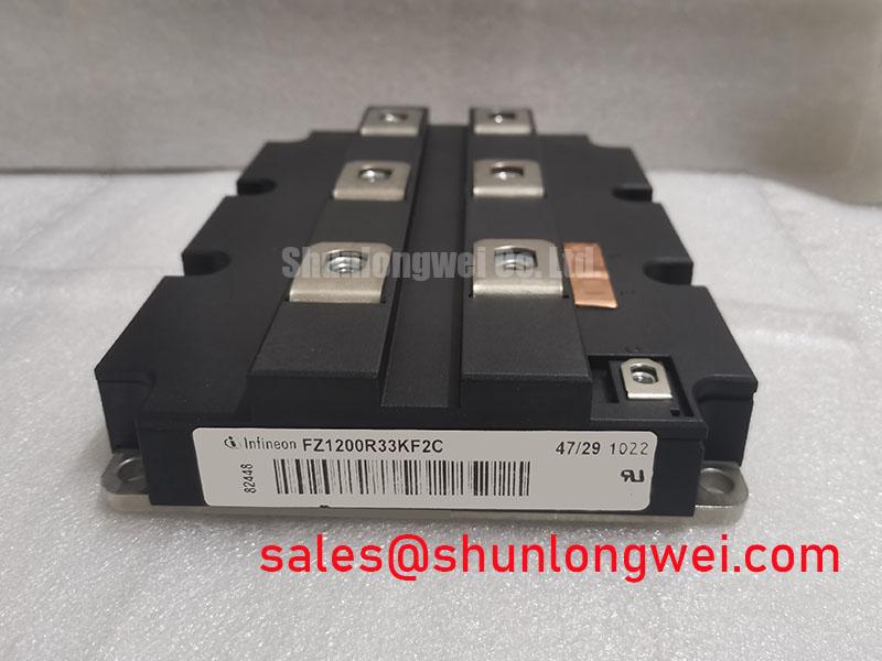
I check terminal screw engagement against the assembly drawing before tightening a busbar onto the FZ1200R33KF2-B5. A screw that bottoms out can appear tight without establishing the intended contact pressure. Check the complete stack, including busbar thickness and specified washers, rather than judging engagement from the screw alone.
Design Consideration: Support the busbar so its mating surface rests naturally against the terminal. Do not use terminal screws to pull a misaligned conductor into position. Check adjacent supports, cable loading, and tool access before assembly; external bending loads can stress terminal connections during vibration and thermal movement. A shifted terminal or distorted housing warrants further inspection, but does not establish a particular internal failure mechanism.
For incoming static checks, I identify collector, emitter, and gate from the terminal diagram before connecting the meter. With the gate held at emitter potential using an appropriate ESD-safe arrangement, compare collector-to-emitter diode-mode readings in both polarities against the documented circuit and a known-good reference under comparable temperature conditions. Parallel circuitry must be isolated where it would influence the reading. A handheld meter provides a screening observation, not verification of the rated blocking voltage.
Bench Tip: Use ESD-safe handling and record cold-state comparison readings before fitting busbars, because connected circuitry can obscure the module’s static behavior.
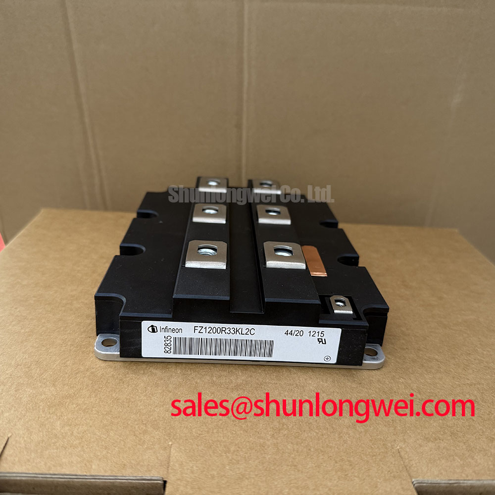
Design Consideration: For an alternative such as FZ1200R33KL2C, compare terminal positions, mounting geometry, switching characteristics, and driver requirements before approving substitution; a similar model designation does not establish direct interchangeability.
Preventing Spurious Faults: Power-Up Shoot-Through Guidelines for FZ1200R33KF2-B5
Check that the gate driver reaches its defined disabled state before the DC link is energized. Design Consideration: Auxiliary-supply startup, undervoltage lockout, controller reset, and enable signals should leave the switching command inhibited throughout startup and shutdown. Establish the required off-state gate bias from the approved device and driver design rather than imposing a generic negative-voltage range.
Trace the gate-drive return to the emitter connection identified in the device drawing. Where a documented auxiliary emitter terminal is provided, keep its driver-return route separate from the load-current path. Shared emitter inductance can alter the effective gate-emitter voltage during current transitions. Verify the actual pin assignment before wiring; terminal appearance alone is not sufficient identification.
Design Consideration: Examine startup waveforms at the gate-emitter connection with suitably rated measurement equipment and a controlled commissioning procedure. Look for unintended excursions during auxiliary-supply transitions and neighboring-switch activity. Reverse-transfer capacitance, commonly designated Cres, describes capacitive feedback; it is not a gate-charge value. Miller-related behavior depends on operating conditions and the complete driver loop. Evaluate any Miller clamp or active collector-voltage clamp as a specific circuit function, not as an assumed module feature.
The Infineon IGBT Modules & Discretes Official Portfolio provides manufacturer-level product context. The separate Infineon Intelligent Power Modules portfolio should not be taken as evidence that this module incorporates a driver or protection controller. Likewise, another topology device such as FZ1200R12KF4 requires its own electrical and driver assessment; it does not establish compatibility with this module’s power stage.
Transient Dynamics & Electrical Design: Preventing Terminal Overheating in FZ1200R33KF2-B5
Place four-wire resistance probes across the intended bolted interface, not across an undefined length of busbar. Design Consideration: Record probe positions, joint temperature, instrument resolution, and assembly condition so subsequent readings remain comparable. De-energize and isolate the equipment before resistance measurements. Treat acceptance resistance as an assembly-specific requirement rather than assigning an unsupported universal micro-ohm limit.
Inspect mating surfaces for contamination, uneven seating, and evidence of movement. Use the specified fastening procedure and approved hardware; additional tightening is not a reliable remedy for every warm terminal. Differences between comparable joints can help prioritize inspection, but should be interpreted alongside current distribution, conductor geometry, and cooling conditions.
Design Consideration: During an authorized energized thermal survey, compare corresponding connections under a stable, recorded load. Reflective metal surfaces and restricted viewing angles can distort apparent temperatures, so thermography should be correlated with electrical measurements and physical inspection. A localized hot region may involve contact resistance, unequal loading, or nearby heat sources; it does not uniquely identify an internal module defect.
The 1200 A official current rating is a device specification, not a terminal-temperature acceptance criterion. When evaluating this module for a utility-scale centralized battery energy storage PCS, designers should assess bidirectional operating states, cooling, current sharing, and converter protection against the applicable device characteristics. That assessment also needs to cover diode conduction and commutation, rather than considering only the commanded IGBT conduction interval.
Assembly Integrity & Layout Architecture: Implementing High-Frequency Commutation Loop Inductance for FZ1200R33KF2-B5
Trace the commutation loop through the local DC-link connection, switching devices, and return conductor before changing busbar geometry. Design Consideration: Keep outgoing and return paths closely coupled where insulation requirements permit, avoiding unnecessary loop area and unequal branch lengths. Mechanical symmetry is useful only when it also produces suitable electrical paths and leaves terminal joints unstressed.
Engineering Calculation: A first-order estimate expresses collector-voltage overshoot as Vpeak ≈ VDC + Lσ × |di/dt|. This relationship explains why connection inductance and switching rate must be evaluated together. Determine acceptable overshoot through measured switching behavior and the 3300 V blocking specification, accounting for the system’s operating envelope rather than selecting an arbitrary inductance target.
Design Consideration: Select snubber capacitance, damping, pulse capability, and placement from the measured transient and circuit losses. Compare waveforms with a consistent probing arrangement so measurement-loop pickup is not mistaken for collector overshoot. Diode reverse recovery can affect ringing and electromagnetic emissions, but a reverse-recovery softness factor cannot be assigned to this model without its characteristic data and test definition.
For insulation checks, distinguish semiconductor blocking voltage from the specified terminal-to-baseplate insulation test. Set the test arrangement, duration, and acceptance criteria from the applicable manufacturer and equipment procedures; do not derive a withstand-test voltage from the collector-emitter rating. Maintain required clearances around busbar edges, fasteners, and chassis boundaries after final assembly.
The Wide Bandgap Revolution article provides comparative switching-technology background, not qualification or lifetime evidence for this Infineon module. For maintenance trending, retain assembly records, thermal observations, and repeatable electrical measurements, then investigate changes against the same operating conditions.