

Content last revised on November 10, 2026
Transient Dynamics & Electrical Design: Retrofit Tuning of Turn-On/Turn-Off on BSM200GA120DN2
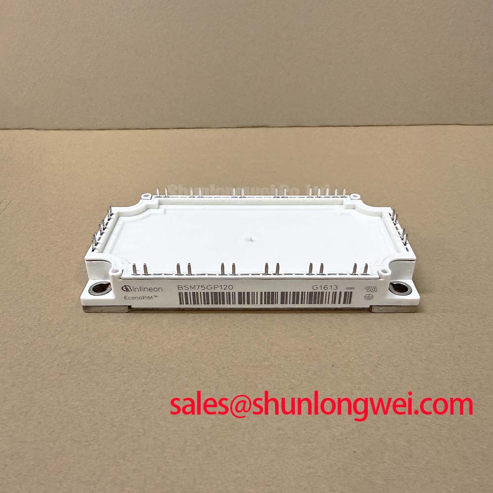
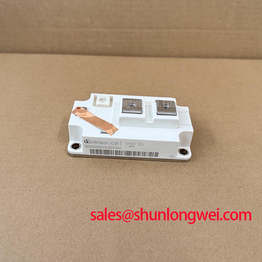
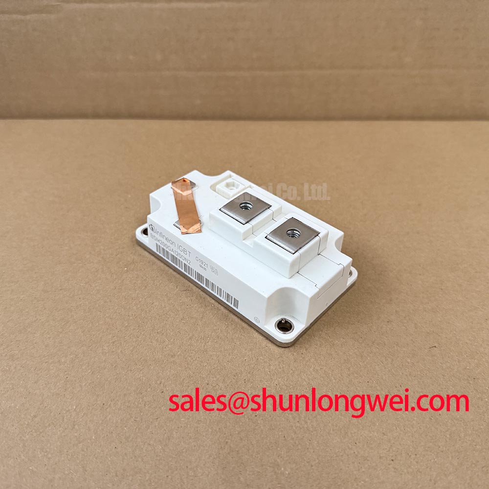
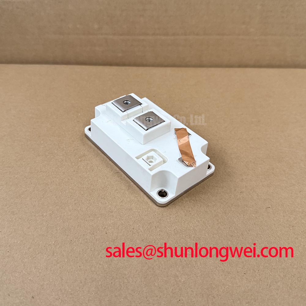
With the DC link discharged and the gate protected against electrostatic charge, identify the collector, emitter, and gate connections before placing a meter across the power terminals. The Infineon BSM200GA120DN2 IGBT module has a 1200 V collector-emitter voltage rating and a 200 A collector-current rating at a case temperature of 80°C—specifications that belong on the incoming inspection record alongside the terminal arrangement and equipment revision.
Other specifications are 2.5 V typical collector-emitter saturation voltage, 2500 V AC isolation voltage, and 1250 W total power dissipation at a case temperature of 25°C. Saturation voltage is an operating-point measurement, not a diode-mode acceptance threshold; the typical value must be read with its datasheet test conditions. Likewise, the isolation rating is a defined test characteristic, not a continuous working-voltage allowance, and the power-dissipation limit is not the heat output expected in service.
Trace the existing driver’s charging and discharging paths before changing either external gate resistor. As a Design Consideration, separate turn-on and turn-off resistance adjustments can help balance switching energy, collector-voltage overshoot, and ringing, but the useful adjustment range depends on driver impedance, interconnect inductance, and the operating load. A mechanically compatible module does not establish electrical drop-in compatibility.
For the cold incoming check, isolate the module sufficiently to prevent the driver, snubber, or parallel power paths from dominating the reading. Check gate-to-emitter behavior without deliberately stressing the gate dielectric. Where the terminal diagram identifies an antiparallel diode, compare its forward-direction meter response and reverse-direction behavior with a known-good reference under the same instrument conditions. Unexpected readings warrant further isolation and inspection; a handheld meter cannot establish full blocking capability or switching performance.
💡 Bench Tip: Keep the gate under ESD control and use the same meter, polarity, and module temperature when comparing cold measurements with a known-good reference.
During controlled switching evaluation, observe gate-emitter voltage at the module terminals together with collector-emitter voltage and current. Short probe connections and suitable differential measurement equipment help distinguish actual oscillation from pickup. Adjust one driver variable at a time and retain the corresponding waveform record. A change that reduces ringing may increase switching energy, so a clean-looking trace alone is not sufficient evidence of an acceptable setting.
Miller coupling deserves particular attention during the opposite switch’s voltage transition. As an Engineering Recommendation, evaluate the driver’s ability to hold the gate off throughout that transition, including supply tolerance and return-path disturbance. The article Evolution of Negative Off-Bias Gate Drive Circuits provides background for this assessment; it does not establish a negative-bias setting for this module. Active clamping also requires coordination with driver behavior and the permitted device operating envelope.
For cross-model comparison, the FZ1800R12KL4C is a separate device to assess against its own electrical and mechanical documentation, not a presumed replacement. Compare circuit configuration, terminal positions, switching characteristics, cooling requirements, and protection coordination before considering any change. A shared voltage class does not make modules interchangeable.
BSM200GA120DN2 Circuit Protection & Reliability: Assessing Thermal Cycling Margins in Braking Applications
Locate the actual braking switch and resistor connections on the equipment schematic before assigning a braking function to the BSM200GA120DN2. The presence of this module does not establish that a braking chopper is integrated into it. As a Design Consideration, braking assessment belongs to the complete energy path: motor regeneration, DC-link capacitance, chopper control, resistor loading, and the cooling arrangement.
Capture DC-link voltage and braking current through the intended deceleration sequence, including repeated operation after the assembly has warmed. Resistor pulse-energy capability and average thermal loading address different constraints. The switching device must also remain within its applicable operating limits during each pulse. Neither the module’s continuous collector-current rating nor its total power-dissipation rating can be substituted for a braking-duty assessment.
Where the equipment includes a phase-controlled rectifier, its conduction angle influences how energy enters the DC link and how charging current is drawn from the supply. That behavior belongs to the front-end controller, not to an intrinsic function of this IGBT module. Engineers should examine line-frequency ripple alongside braking-related bus excursions so that capacitor charging effects are not mistaken for chopper instability. Harmonic performance remains a system-level measurement.
An RC snubber can influence local transient behavior, but its selection should follow the measured ringing path and repetitive energy burden. As an Engineering Recommendation, inspect existing snubber components, their connections, and signs of thermal deterioration before changing values. Shortening the relevant commutation path may address a different problem from adding damping; neither action should be judged solely by a single unloaded waveform.
The BSM100GAL120D can be documented separately when reviewing complementary switching positions elsewhere in a power-conversion assembly. Its role must follow the schematic and its own device specifications; it should not be classified as a front-end rectifier simply because it appears near the input stage. During repair, keep the identity and test record of each power position distinct.
Thermal cycling is best approached here through repeatable operating observations: case-temperature trends, cooling-system condition, braking repetition, and recovery between load events. These measurements support troubleshooting without implying a service-life prediction. Infineon’s article on CoolSiC with .XT technology discusses a different technology context; its packaging discussion must not be treated as evidence that the BSM200GA120DN2 incorporates .XT technology or shares its reliability results.
Benchtop Waveform Tuning: Baseplate Contact and Screw Mounting on BSM200GA120DN2
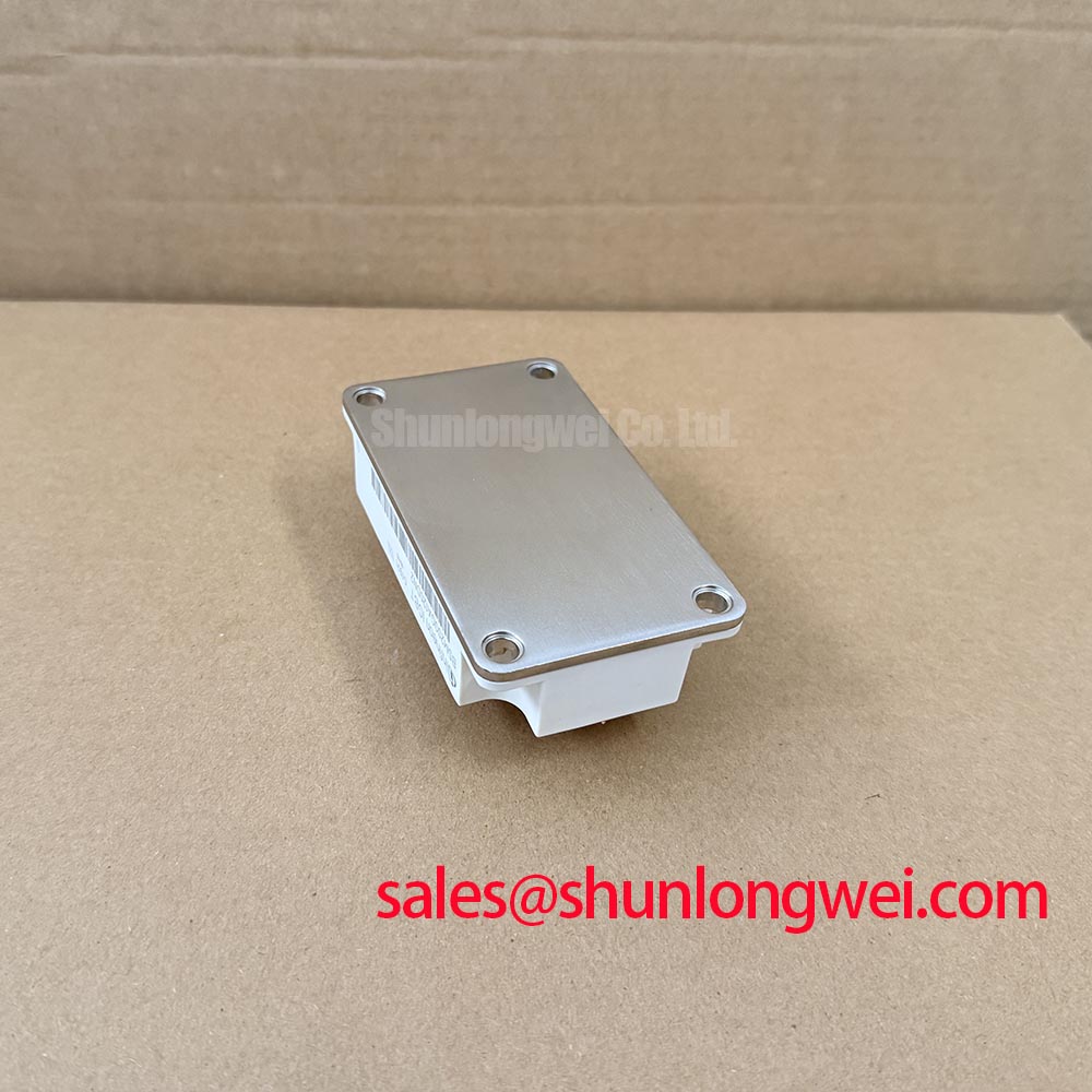
Inspect the heatsink contact surface and mounting hardware before tightening the module into place. As a Design Consideration, uneven support, contamination, or displaced thermal interface material can produce inconsistent heat transfer and mechanical loading. Baseplate curvature should be evaluated against the applicable mechanical drawing rather than corrected by force or assumed to be a defect.
Use the module’s mounting instructions and the selected interface material’s application guidance to establish the assembly process. Thermal interface thickness is not a universal setting: the required bond line depends on surface geometry, material behavior, and mounting pressure. Apply the material consistently and examine the contact pattern during process qualification. Excess material around an edge does not, by itself, prove either satisfactory coverage or an internal void.
Bring mounting screws into engagement progressively using the specified sequence and tightening requirements for the actual package. Avoid using a screw to pull a visibly misaligned assembly into position. Terminal connections should likewise meet the module without imposing avoidable bending loads. A repeatable assembly record should identify the heatsink preparation, interface material, fastener arrangement, and tightening procedure rather than relying on an undocumented workshop habit.
The 1250 W at 25°C case temperature dissipation specification is a boundary condition, not a heatsink selection shortcut. During evaluation, relate measured losses and case temperature to the cooling path and the manufacturer’s thermal limits. As an Engineering Recommendation, compare temperatures at consistent locations after equivalent load sequences; a different measurement location or airflow condition can obscure whether a mounting change actually improved heat transfer.
Electrical switching checks should follow a stable mechanical and thermal setup. A colder test can conceal behavior that appears after heating, while repeatedly changing the mounting arrangement makes waveform comparisons difficult to interpret. Record the temperature state with each switching capture and inspect cooling performance before attributing a temperature-dependent fault entirely to gate resistance.
For incoming insulation screening, separate the specified isolation test from semiconductor blocking tests and from an equipment-level insulation assessment. Fixture connections, test duration, ramp behavior, and acceptance criteria must follow the applicable manufacturer procedure. An arbitrary workshop withstand test can stress the assembly without producing a meaningful acceptance result. The 2500 V AC rating should therefore be recorded with its specified test conditions, not converted into a claimed installation clearance or continuous insulation margin.
Preventing Spurious Faults: PCB Symmetry and Driver-Return Guidelines for BSM200GA120DN2
Route the gate-driver return so that load-current voltage drops do not unnecessarily enter the gate-control loop. This is a Design Consideration for the surrounding switching circuit, not evidence that the BSM200GA120DN2 contains a dual-IGBT arrangement or a dedicated Kelvin-emitter terminal. Terminal functions must come from the actual connection diagram; a control return should not be assigned to an unverified pin.
Where the circuit provides a separate control-return connection, preserve its separation from the high-current emitter path until the intended reference point. Where it does not, examine shared connection impedance and place the driver reference deliberately. Geometric symmetry can help make comparable switching positions behave consistently, but visual symmetry alone cannot compensate for different current paths, connector resistance, or unequal driver-loop lengths.
When a protection signal appears during switching, capture the local gate-emitter waveform and the relevant sensing signal on a common time reference. Distinguish a real collector-current event from a disturbed protection reference before changing thresholds. Inspect sensing connections, blanking behavior, driver-supply disturbance, and probe placement. Intermittent trips can have several contributing causes, so disabling protection to obtain a cleaner run is not a valid diagnostic endpoint.
For a bootstrap-powered driver, examine supply behavior over the actual switching pattern, especially when refresh opportunities are restricted. As an Engineering Recommendation, assess capacitor charge balance, charging-path recovery, and undervoltage behavior together. These checks concern the installed driver circuit; they do not establish a bootstrap capacitor value or recovery specification for the IGBT itself.
In an electric forklift or material-handling traction assessment, the battery voltage, current duty, controller topology, and existing power-device technology should determine compatibility—not the availability of a high-voltage module. Infineon’s OptiMOS low-voltage MOSFET portfolio provides a separate technology reference for such comparisons, not a direct replacement recommendation. For the BSM200GA120DN2 installation under evaluation, close the test record with terminal-referenced waveforms, driver-return routing, protection response, and the temperature conditions under which those measurements were obtained.