Content last revised on September 10, 2026
BSM50GD120DN2G Circuit Protection & Reliability: Calibrating High-Frequency Common-Mode Bearing Current
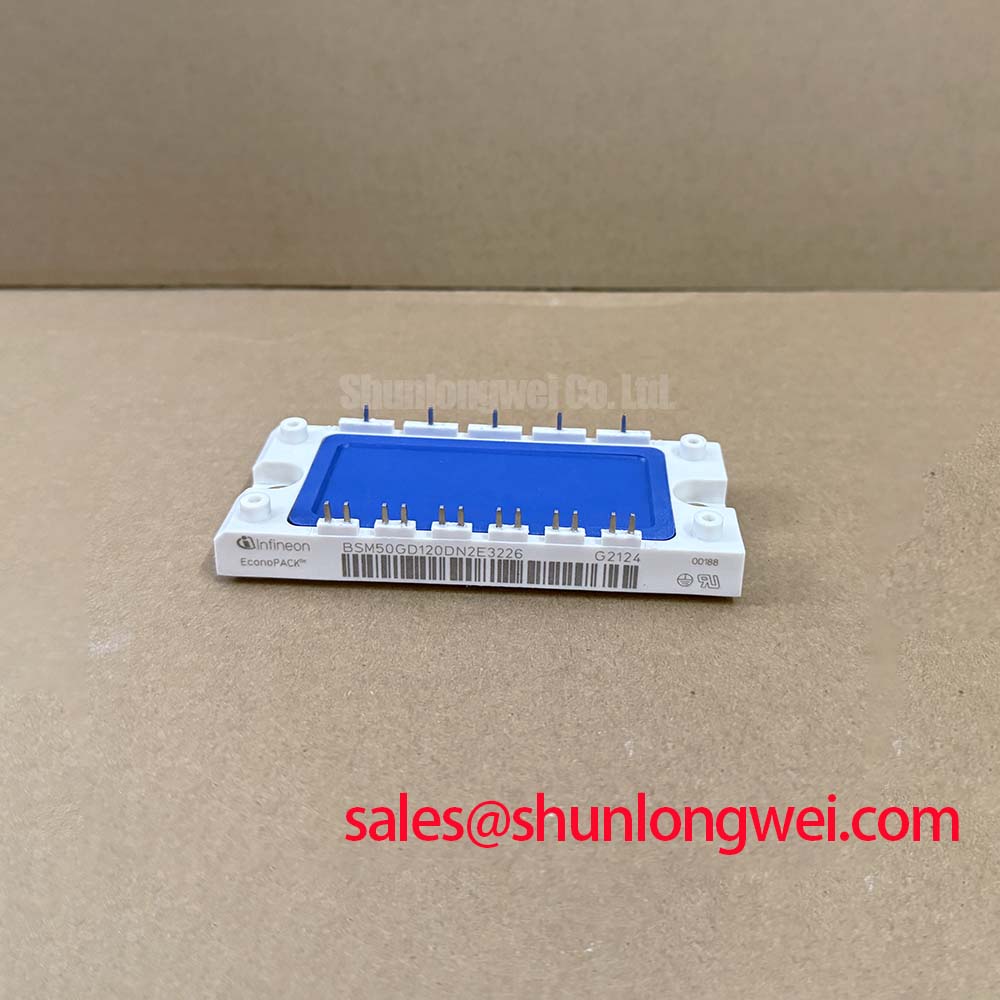
At the service bench, isolate the DC link, inspect the package and terminals, then compare cold-state impedance readings with a known-good assembly before applying any gate signal. The BSM50GD120DN2G is an Infineon IGBT module specified with a 1200 V collector-emitter voltage and 78 A continuous DC collector current at Tc = 25°C. These are Official Specification values and should be checked against the converter’s measured electrical limits before replacement.
| Manufacturer | Infineon |
| Product type | IGBT module |
| Collector-emitter voltage, VCES | 1200 V at Tj = 25°C |
| Continuous DC collector current, IC | 78 A at Tc = 25°C |
| Collector-emitter saturation voltage, VCE(sat) | Typical 2.5 V, maximum 3.1 V at IC = 50 A, VGE = 15 V, Tj = 25°C |
| Gate-emitter voltage, VGE | ±20 V |
| Total power dissipation per IGBT | 400 W at Tc = 25°C |
| Thermal resistance, RthJC | ≤ 0.35 K/W per IGBT |
| Operating junction temperature | −40°C to +150°C |
Field Diagnostics & Commissioning: Baseplate Convexity Compensation and Screw in BSM50GD120DN2G Topologies
Long motor leads can behave as a transmission line rather than a simple resistive connection. Reflections caused by impedance mismatch can raise switching-node overshoot, increase common-mode voltage, and contribute to bearing-current stress in motor-driven equipment. The resulting waveform is determined by the DC-link voltage, cable construction, motor impedance, switching edge, termination, and grounding arrangement; it is not an independent rating of the BSM50GD120DN2G.
For an electric forklift or material-handling traction inverter, examine the motor cable shield termination, chassis bonding, return-current path, and the physical distance between the inverter and motor. Designers should minimize the parasitic loop area and verify collector-emitter overshoot directly with a suitable differential probe during switching tests. Output filters, common-mode chokes, or dv/dt networks should be selected from measured waveform data and the motor manufacturer’s insulation limits, with losses and resonance checked across the complete operating range.
The module’s official VCES rating is 1200 V, but the system engineer must verify the actual peak voltage at the terminals rather than treating the rating as a target operating point. A failed unit should be checked alongside the gate driver, snubber network, DC-link film capacitors, cable shield, and motor insulation. The Infineon Infineon IGBT Modules Overview provides useful manufacturer-level context for module integration, while application-specific filter validation remains the responsibility of the equipment designer.
Thermal inspection begins with the mounting surface, not the oscilloscope. Remove contamination, check the heatsink for burrs or local high spots, and confirm that the baseplate sits evenly before tightening. Thermal interface material should form a uniform, continuous contact layer without trapped air, excessive spread, or dry areas. The correct material and application method must follow the relevant assembly documentation and the actual heatsink finish.
Use a crosswise, progressive tightening sequence so the baseplate is not pulled into a distorted position. The required torque is system and fastener dependent; use the applicable Infineon assembly instruction and the screw manufacturer’s data rather than assigning a universal value to this module. After commissioning, compare case temperature, phase-current balance, and switching waveforms under the same load. The specified RthJC ≤ 0.35 K/W per IGBT is an Official Specification under its stated thermal conditions, not a complete heatsink performance guarantee.
Switching-frequency changes alter semiconductor losses, gate-driver losses, and cooling demand. At higher operating frequency, designers should reassess thermal impedance, airflow, coolant condition, and current derating instead of carrying over a low-frequency load assumption. The official 400 W total power dissipation per IGBT at Tc = 25°C must be interpreted with the complete thermal path and junction-temperature limit of −40°C to +150°C. For a suspected thermal fault, log case temperature at multiple operating points and inspect whether the temperature rise follows load current, switching activity, or an uneven mounting interface.
⚠️ Field Alert: Disconnect the DC link and gate-drive supply before unplugging control wiring, and confirm the module has reached a safe measured voltage before handling terminals.
BSM50GD120DN2G Operational Boundaries: Evaluating Auxiliary Emitter Return Trace Separation Limits
Gate-drive reference routing deserves the same attention as the power path. Shared impedance in the emitter return can convert high-current switching transients into an apparent gate-voltage disturbance. This may produce ringing, false turn-on, uneven current sharing, or unexplained driver protection events. The correct evaluation method is to measure the gate-emitter waveform at the module terminals with a short, low-inductance probe connection and compare it with the driver-side signal.
Keep the gate-drive return physically distinct from the high-current emitter path wherever the module and schematic permit that arrangement. Minimize the commutation loop, avoid routing the gate signal alongside the collector bus, and place gate resistance and any clamp components according to the driver topology. The required separation and copper geometry are Design Considerations determined by current, edge rate, insulation structure, and board construction; they should be confirmed through double-pulse or inverter switching tests.
The gate-emitter limit for this device is ±20 V according to the supplied Official Specification. That limit does not define a preferred drive waveform or guarantee immunity from parasitic coupling. If cold-state tests are normal but the module trips only under load, inspect the gate loop, auxiliary emitter reference, driver supply decoupling, and probe technique before condemning the power module. For an alternative evaluation within the same voltage class, engineers may compare the application requirements with BSM75GD120DLC; electrical, mechanical, thermal, and gate-drive compatibility must be verified independently.
BSM50GD120DN2G Operational Boundaries: Evaluating High dv/dt Cross-Conduction Shoot-Through Limits
Cross-conduction investigation should start with simultaneous gate-waveform capture on the complementary switches. A high dv/dt transition can couple through the device’s parasitic capacitances and disturb the opposite gate. The result depends on the driver’s sink capability, propagation delay, gate-loop inductance, dead-time strategy, layout, and DC-link commutation path. It should not be reduced to a single assumed voltage or timing value.
Active Miller clamp circuitry can help hold the inactive gate near its intended state when the switching node moves rapidly, provided the driver supports the required function and the clamp connection is routed with low impedance. Negative gate bias is another possible Design Consideration, but its permitted value must come from the selected driver and the module’s validated gate-drive conditions. Do not apply a negative bias by assumption; verify the complete gate-emitter waveform, including ringing, during turn-off and fault events.
Desaturation protection and soft turn-off should be coordinated with the gate driver, current-sensing path, isolation barrier, and short-circuit response. The supplied module data confirms VCE(sat) typical 2.5 V and maximum 3.1 V at IC = 50 A, VGE = 15 V, Tj = 25°C; these values support conduction assessment under the stated test conditions but do not establish a universal short-circuit duration or safe-operating-area window. Any short-circuit protection decision requires validated switching tests at the intended DC-link voltage, current, temperature, and gate-drive conditions.
In bidirectional battery converter or traction architectures, review both motoring and regenerative operation. Power flow reversal changes which devices conduct, how heat is distributed, and how the gate driver responds to abnormal current. Designers should verify current sharing, thermal cycling, dead-time behavior, and line-to-line fault response on the assembled converter. A related topology reference can be reviewed through BSM75GB120DN2, while technology selection for other 1200 V switching positions should remain based on independently verified electrical and thermal requirements. The The 1200 V CoolSiC™ MOSFET Advantage in Three article may assist with broader topology comparisons without changing the specified limits of the BSM50GD120DN2G.