

Content last revised on September 10, 2026
Planar Symmetrical Busbar Geometry: Achieving L_sigma < 20nH to Protect Silicon Junctions
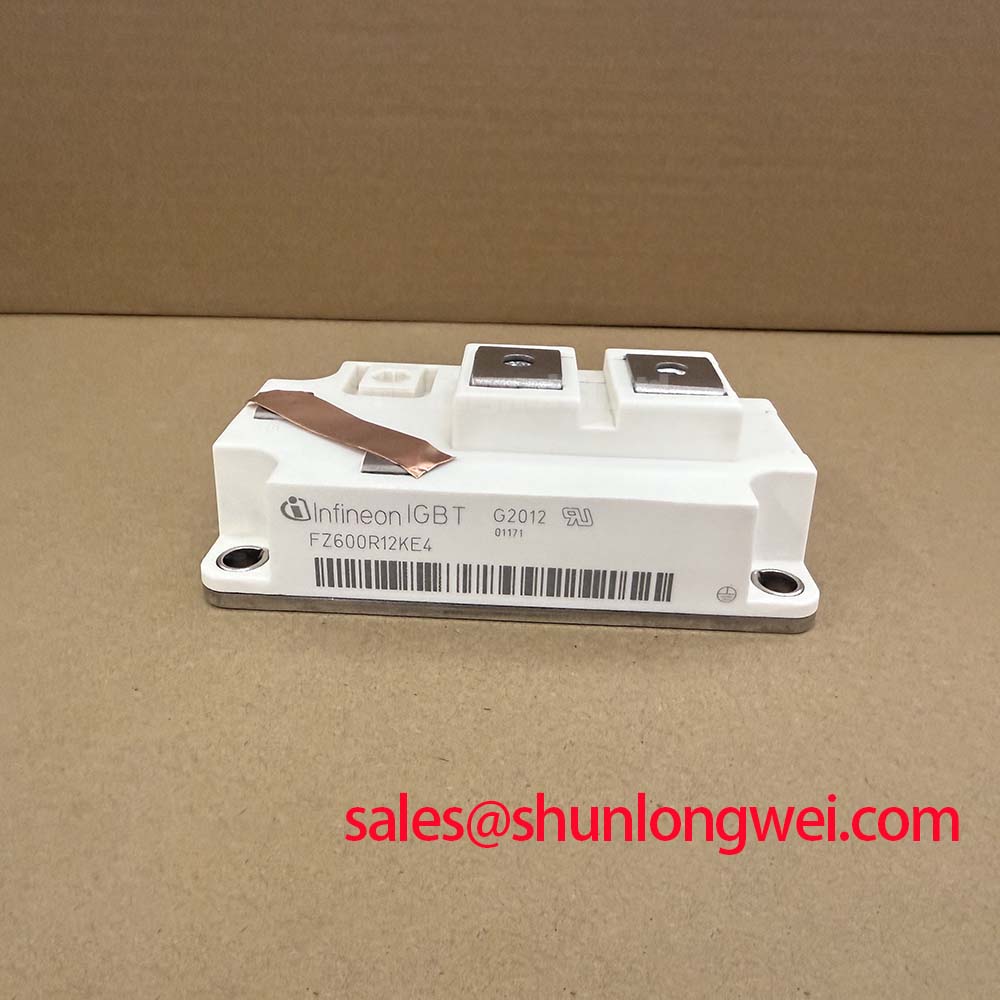
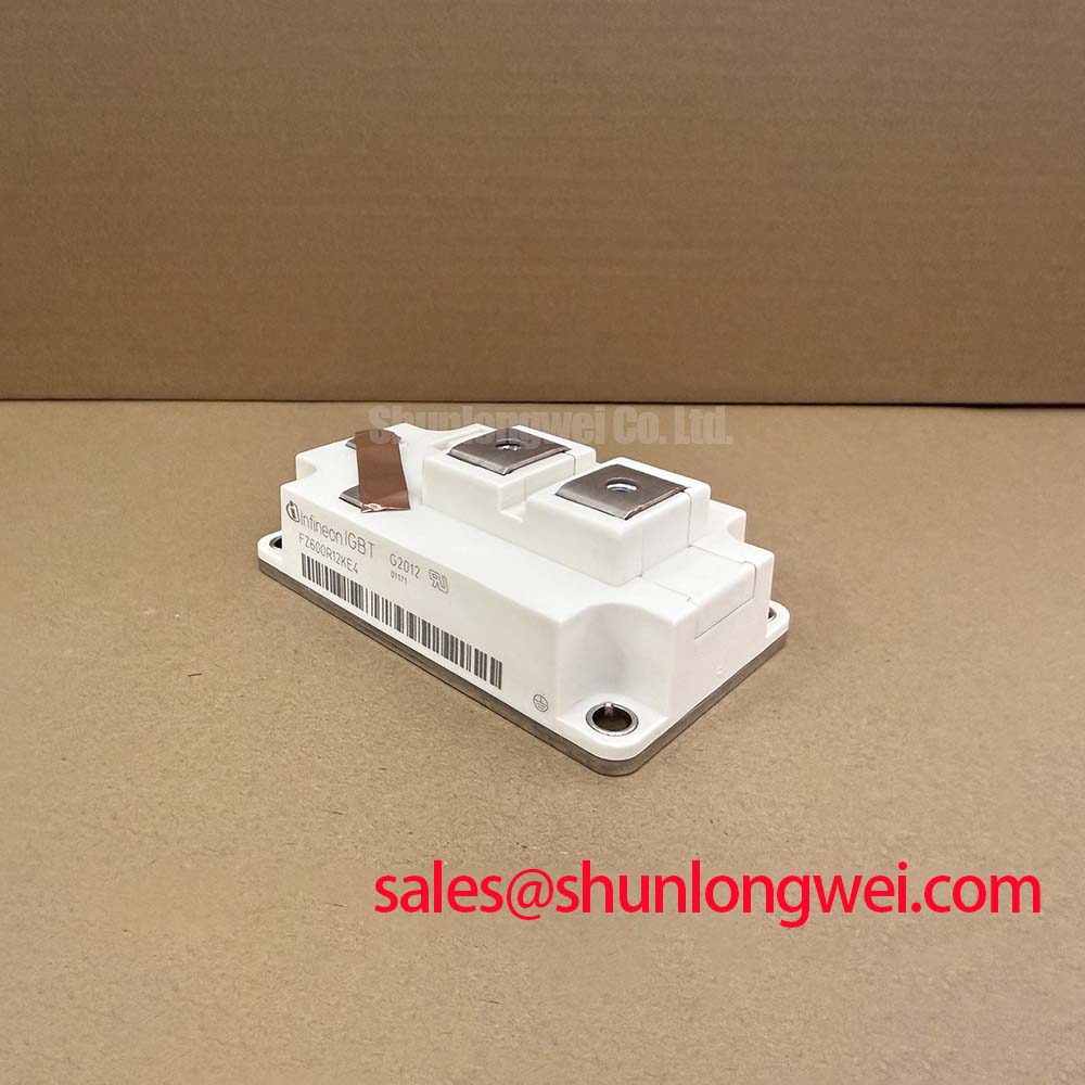
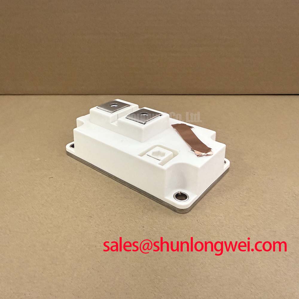
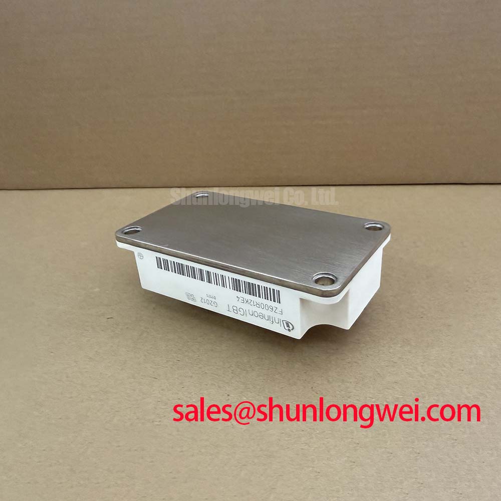
Field emergency response in utility-scale 1500V central and string solar inverters frequently uncovers catastrophic IGBT failure modes traceable directly to excessive DC-link stray inductance. In high-power inverter topologies, the Infineon FZ600R12KE4 operates as a critical switching building block, rated for a collector-emitter breakdown voltage of VCES = 1200V and a continuous collector current of IC = 600A (with a repetitive peak current ICRM = 1200A). During hard switching turn-off events under fault conditions, the rate of current change (di/dt) can easily exceed 3000 A/µs. The resulting induced turn-off overvoltage spike across the silicon die follows the fundamental relationship:
Vpeak = VDC + Lσ × (di/dt)
In a split-rail or multi-level solar inverter configuration with an intermediate DC-link bus sitting at 800V to 900V, an unmitigated parasitic inductance (Lσ) of just 40nH will generate a transient overvoltage surge exceeding 120V to 150V, driving the collector-emitter voltage beyond the absolute maximum 1200V ceiling. This instantly triggers dynamic avalanche breakdown and subsequent thermal runaway across the IGBT chip area.
| Parameter | Symbol | Official Factory Value | Field Diagnostic Tolerance / Limit |
|---|---|---|---|
| Collector-Emitter Breakdown Voltage | VCES | 1200V (Tvj = 25°C) | Absolute maximum rating; never exceed under turn-off peak |
| Continuous DC Collector Current | IC | 600A (TC = 80°C) | Derate linearly at elevated baseplate temperatures |
| Repetitive Peak Collector Current | ICRM | 1200A (tp = 1ms) | Current limit for instantaneous short-circuit desaturation |
| Collector-Emitter Saturation Voltage | VCE(sat) | 1.7V typ. (Tvj = 150°C, IC = 600A) | Measure across power terminals; drift indicates junction aging |
| Gate Threshold Voltage | VGE(th) | 5.8V typ. (Tvj = 25°C) | Gate triage threshold: <5.0V or >6.5V indicates gate degradation |
| Thermal Resistance (Junction-to-Case) | RthJC | 0.045 K/W per IGBT | Requires strict thermal interface material control |
To restrict total loop inductance (Lσ) below 20nH, power stage retrofits and field rebuilds must utilize symmetrical, laminated planar busbars. By placing positive and negative copper conductor plates parallel to each other with a dielectric insulation layer thinner than 0.5mm, opposing magnetic flux lines cancel out most of the internal loop inductance. Snubber film capacitors with equivalent series inductance (ESL) under 10nH must be positioned directly across the DC terminals of the 62mm Standard Baseplate package. For systems requiring alternative voltage blocking ratings or different converter configurations, the related FZ600R65KE3 serves as a baseline comparison for higher voltage architectures.
When selecting semiconductor protection fuses, the clearing I2t integral of the high-speed fuse must remain strictly below the maximum rated rupture energy of the module casing to prevent catastrophic package explosion during phase-to-phase short circuits.
Dynamic Gate Impedance Control for Robust Phase-Leg Dead-Time Operation
In high-power bridge topologies, false turn-on via dynamic dv/dt displacement currents represents one of the most common causes of bridge-arm shoot-through. When the opposing complementary IGBT in a half-bridge switch leg turns on at high switching speeds (dv/dt up to 5 to 10 kV/µs), the rapid rise in collector-emitter voltage across the non-conducting FZ600R12KE4 couples charge directly through the internal gate-collector Miller capacitance (Cres). This creates a parasitic displacement current:
iMiller = Cres × (dv/dt)
If this current flows through the external turn-off gate resistance without adequate damping, the voltage developed across the gate-emitter terminals can easily exceed the typical gate threshold voltage VGE(th) = 5.8V, inducing spurious cross-conduction. To eliminate this vulnerability, the gate driver design must implement active dynamic gate impedance control. A dedicated low-impedance Active Miller Clamp circuit short-circuits the gate path to the negative supply rail once VGE drops below 2.0V during turn-off.
Furthermore, applying a robust negative gate bias voltage between -5V and -15V during the off-state guarantees an adequate noise margin against spurious threshold crossings. The peak output current capability of the isolated gate driver must satisfy the dynamic charge requirements of the gate loop:
Ig(peak) = (VGE(on) - VGE(off)) / (Rg(ext) + Rg(int))
For detailed switching dynamics and gate drive impedance optimization guidelines, refer directly to official platform resources including the Infineon IGBT Modules & Discretes Official Portfolio.
Phase-leg dead-time configuration must be tuned precisely: setting dead-time under 2.0µs risks overlapping conduction during diode reverse recovery tail states, while setting it beyond 5.0µs introduces excessive freewheeling diode conduction losses, degrading overall inverter efficiency and generating thermal hot spots across the anti-parallel diode dies.
Baseplate Convexity Compensation and Screw Tightening Sequence Guidelines
The thermal path of the FZ600R12KE4 relies entirely on its standard 62mm copper baseplate. The factory specification establishes a thermal resistance from junction to case of RthJC = 0.045 K/W per IGBT switch. In field environments, achieving this specified thermal resistance depends strictly on mechanical mounting precision and thermal interface material (TIM) distribution.
Power module baseplates are manufactured with a defined engineering convexity (pre-bow). When mounted onto a machined heatsink surface, tightening the mounting screws forces the baseplate to flatten, creating optimal, uniform pressure across the central ceramic Direct Bonded Copper (DBC) substrate where the silicon chips are concentrated.
⚠️ Field Alert: Never apply thermal grease with a thickness exceeding 100µm. Excessive paste layer thickness increases contact thermal resistance exponentially, leading to rapid overtemperature failure under heavy solar peak hours. Apply a uniform 50µm to 80µm layer using a precision notched squeegee or screen stencil. Ensure heatsink surface flatness deviates by less than 20µm per 100mm, with a surface roughness (Rz) below 6.3µm.
To avoid fracturing internal ceramic substrates and ensure uniform thermal dissipation, adhere strictly to the two-step crisscross tightening procedure:
- Step 1 (Pre-tightening): Finger-tighten all M6 mounting screws, then use a calibrated torque wrench to apply an initial seating torque of 0.5 to 1.0 N·m in a diagonal crisscross sequence (1-4-2-3).
- Step 2 (Final Torque): Apply the final mounting torque of 3.0 to 6.0 N·m following the same diagonal pattern. Allow 15 minutes for the TIM to spread under clamping pressure, then verify torque retention.
- Terminal Connections: Fasten the main M6 power busbar connections to 2.5 to 5.0 N·m. Excessive torque on power terminals stresses internal solder joints, causing early micro-crack propagation under heavy thermal cycling.
Under elevated ambient operational temperatures inside solar combiner enclosures (often exceeding 50°C), derating the Pulse-Width Modulation (PWM) switching frequency (fsw) from 8kHz down to 2kHz to 3kHz significantly reduces dynamic switching losses, protecting the silicon junction from exceeding its 150°C limit during peak irradiance windows. Comprehensive failure diagnostics, baseplate visual wear patterns, and bench testing procedures are detailed in the Field Engineer’s Handbook.
Common-Mode Transient Immunity (CMTI > 100kV/us) in Harsh Industrial Environments
Utility-scale photovoltaic installations operate under aggressive common-mode electrical stress. Rapid switching transitions of high-voltage phase legs couple displacement currents through parasitic capacitance between the inverter electronics, floating DC rails, and the grounded chassis. Gate driver circuits controlling the FZ600R12KE4 must provide reinforced galvanic isolation (>5kV) and a Common-Mode Transient Immunity (CMTI) exceeding 100kV/µs to prevent spurious gate signals and erratic PWM modulation.
Long AC output cables running from the central inverter to the step-up transformer act as transmission lines. High-frequency voltage pulses with steep rise times create transmission line reflections, doubling the voltage peak (2x surge) at motor terminals or transformer primary windings. To suppress these reflected wave spikes, field engineers must deploy dV/dt output filters or tuned sinusoidal LC filters at the inverter output stage.
For in-depth analysis of high-speed switching dynamics and parasitic oscillation suppression in medium-to-high power converters, consult the Infineon TRENCHSTOP™ IGBT3 engineering literature.
Field Diagnostic Triage Routine
When an inverter trips on desaturation or DC bus overcurrent, perform this immediate step-by-step bench inspection before powering the system back up:
- Visual Inspection: Check the 62mm package housing for micro-cracks, resin discolouration, bulging silicone gel, or soot marks near the power terminals.
- Gate Isolation Triage: Set a high-accuracy digital multimeter to resistance mode (MΩ range). Measure between the auxiliary Gate and Emitter pins. A reading below 10MΩ indicates dielectric gate oxide punch-through; replace the module immediately.
- Collector-Emitter Short-Circuit Test: Measure resistance between the collector (C) and emitter (E) terminals in both directions. Any low-impedance reading (<100kΩ) confirms silicon punch-through or thermal melt failure.
- Freewheeling Diode Check: Switch the multimeter to Diode Test mode. Verify the forward voltage drop (VF) of the integrated anti-parallel diode. A normal diode reads between 0.35V and 0.65V at room temperature. A reading of 0.00V indicates an alloyed short, while "OL" in both polarities indicates an open-circuit bond wire lift-off.