Content last revised on September 13, 2026
BSM150GB170DN2 Operational Boundaries: Evaluating Regenerative DC Bus Voltage Surge Dissipation Limits
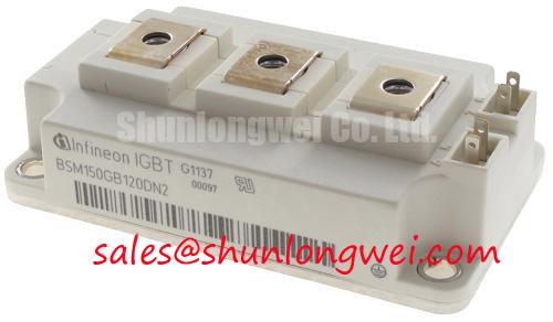
Begin a field replacement check by isolating the traction inverter, confirming the original nameplate data, and inspecting the module body, terminals, mounting surface, and visible insulation barriers before applying any test voltage. The supplied factory parameters identify BSM150GB170DN2 as an Infineon IGBT Module rated at 1700 V and 150 A. These are official specification values supplied for this product page; they do not by themselves define the allowable regenerative pulse, short circuit duration, switching frequency, or cooling performance.
| Parameter | Specified value | Engineering status |
|---|---|---|
| Manufacturer | Infineon | Product identification |
| Part number | BSM150GB170DN2 | Product identification |
| Voltage rating | 1700 V | Official factory specification |
| Current rating | 150 A | Official factory specification |
| Package | Module | Official factory specification |
In a regenerative braking branch, the switching device and ballast resistor must be evaluated as one energy path. During motor deceleration, the inverter control system determines whether energy returns to the supply, charges the DC link, or is diverted through a braking chopper and resistor. The 1700 V voltage rating is an electrical boundary for the semiconductor, not a permission to operate the DC bus at that value. Designers should verify the actual bus voltage, transient overshoot, regenerative energy per event, repetition rate, resistor thermal capacity, and protection response using the complete traction inverter design.
The relevant assessment is a transient energy and voltage study rather than a simple comparison between bus voltage and the label rating. The IGBT current path, freewheel diode path, braking resistor, DC link, wiring inductance, gate driver, and control timing all influence the peak stress. The supplied data does not include ITSM, repetitive peak current, short circuit withstand time, junction temperature limits, transient thermal impedance, or safe operating area curves. Those values must be taken from the applicable Infineon documentation before a braking pulse is approved.
For a high speed rail or heavy freight locomotive traction inverter, technicians should record the DC link waveform during acceleration, motoring, regenerative braking, and emergency stop conditions. An oscilloscope with a correctly rated differential voltage probe can reveal whether a fault is associated with bus rise, switching overshoot, control timing, or a damaged power path. If a ballast resistor is present, inspect its connections, cooling route, contactor operation, and resistor temperature feedback rather than assigning the fault to the IGBT alone.
Clearance and creepage around the high voltage power loop should be verified against the applicable equipment insulation design and operating environment. Rail equipment can introduce vibration, contamination, altitude variation, and long cable runs, so the system designer must confirm the final insulation coordination and environmental requirements. The Infineon EasyPACK™ power semiconductor reference material can provide general manufacturer context, but it should not be treated as a specification for this particular module.
Field Diagnostics and Commissioning: Baseplate Convexity Compensation and Screw in BSM150GB170DN2 Topologies
After electrical isolation, compare the replacement position with the removed unit and check that the baseplate, heatsink, insulator, busbar, and gate connections are mechanically compatible. A module package designation alone does not confirm terminal pitch, hole pattern, internal circuit topology, diode arrangement, or control interface. The system integrator should verify these items against the original equipment drawing and the applicable product documentation before installation.
The thermal interface is a frequent source of avoidable field failure. The heatsink should be clean, flat within the equipment manufacturer’s stated tolerance, and free from burrs or trapped particles. Apply the selected thermal interface material as a uniform, controlled layer according to its supplier instructions. The 50 to 100 micrometre range is a general integration consideration, not an official BSM150GB170DN2 factory parameter. The correct thickness depends on the material, surface finish, pressure distribution, and heatsink geometry.
Baseplate curvature should be checked with suitable mechanical inspection equipment when uneven contact is suspected. Do not use excessive screw force to compensate for a distorted heatsink. A bowed mounting surface can leave air pockets beneath the baseplate, producing local thermal resistance and uneven pressure. Install fasteners progressively in a cross pattern so the baseplate seats evenly, then apply the torque specified by the equipment drawing, fastener grade, and module documentation. The module rating does not establish a universal screw torque.
⚠️ Field Alert: Disconnect and verify the DC link is discharged before touching power terminals, gate wiring, or mounting hardware.
Commissioning should include a visual inspection of the interface layer, terminal alignment, busbar stress, and gate lead routing. After low energy checks, monitor collector emitter voltage, gate emitter voltage, phase current, heatsink temperature, and cooling airflow during controlled operation. A rising temperature trend may involve switching losses, conduction duty, cooling restrictions, interface resistance, or control timing. It should be investigated through measurements rather than attributed to one component without waveform and thermal evidence.
Switching frequency and ambient temperature directly affect the available thermal margin, but the supplied product data does not specify a derating curve for the 2 kHz to 16 kHz range. Engineers should obtain the switching loss curves, transient thermal impedance network, maximum junction temperature, and case temperature conditions before selecting an operating point. Airflow requirements are system determined and depend on heatsink resistance, duct design, filter loading, altitude, and enclosure temperature. A replacement test should therefore reproduce the actual cooling arrangement instead of relying on a bench fan.
Preventing Spurious Faults: Suppressing Cres Induced Gate Voltage Spikes in BSM150GB170DN2
Unexpected gate movement during a fast collector voltage transition can produce false turn on, cross conduction, or protection trips. The mechanism may involve common emitter inductance, capacitive coupling, gate loop impedance, driver return routing, probe loading, or an unsuitable dead time. The term Cres should be assessed within the complete switching network because the supplied factory information does not provide a switching capacitance value or a guaranteed dv/dt immunity limit for this page.
Begin diagnosis with a properly referenced differential gate measurement at the module terminals, not at a distant driver connector. Compare the command waveform with the actual gate emitter waveform during both turn on and turn off. Inspect the gate resistor path, driver supply stability, return conductor, isolation barrier, and auxiliary protection components. Ringing that appears only after the power bus is connected may indicate a parasitic coupling or layout interaction, while a distorted waveform under all conditions may point toward the driver, wiring, or module condition.
A low impedance gate loop is a design consideration for controlling parasitic inductance and limiting oscillation. Gate damping, ferrite elements, active Miller clamp circuitry, and separate turn on and turn off paths may be evaluated when supported by the selected driver architecture. Negative gate bias is also a system design option, but the −5 V to −15 V range is not an official parameter supplied for BSM150GB170DN2. The gate driver manufacturer’s absolute maximum ratings, insulation limits, turn off behaviour, and module documentation must govern the final choice.
When long motor cables are connected, measure the gate waveform and phase voltage under the same cable length and termination arrangement used in service. Cable impedance and reflection can increase voltage stress at the motor or inverter terminals, and an approximately two-times peak, if observed, should be investigated as a possible transmission-line effect requiring system measurement. Common countermeasures can include an appropriate output filter, controlled switching speed, cable termination strategy, and layout improvement, but the selected solution must be validated against motor insulation, leakage current, EMC behaviour, and semiconductor switching loss.
For technical background on switching behaviour and industrial drive integration, engineers can review Unlocking Efficiency in Industrial Drives. This reference supports general design discussion and does not replace the product specific electrical and thermal documentation required for commissioning.
Field Diagnostics and Commissioning: DC Link Capacitance Bank Layout and Low ES in BSM150GB170DN2 Topologies
Inspect the DC link capacitor bank, laminated busbar, snubber connections, and braking branch before condemning the power module. Loose joints, unequal conductor lengths, cracked capacitor terminals, and a remote capacitor bank can increase commutation overshoot. In practical analysis, the peak voltage is influenced by the DC bus, stray inductance, and current change rate, so the switching loop must be evaluated as a physical structure rather than as an ideal schematic.
Place the high frequency decoupling path as close as the equipment insulation and mechanical design allow, while keeping the forward and return conductors closely coupled. A symmetrical planar busbar generally reduces loop area and helps balance current sharing between parallel paths. The target of less than 25 nH is not an official BSM150GB170DN2 specification and should not be adopted as a universal pass or fail limit. The system engineer should determine an acceptable inductance and verify peak voltage with calibrated probing during the intended switching conditions.
Snubber capacitance and damping resistance must be selected from measured ringing frequency, energy, pulse repetition, capacitor pulse capability, and temperature rise. Increasing capacitance without checking turn on current and switching loss can move stress into another part of the circuit. Check capacitor ESR, mounting inductance, discharge provisions, and insulation spacing. If the DC link uses multiple capacitor groups, compare their physical current paths and terminal temperatures under load.
Low impedance is useful only when it is achieved without compromising service clearance, vibration resistance, insulation coordination, or maintainability. Technicians should capture the voltage directly at the module power terminals and compare it with the voltage measured at the capacitor bank. A significant difference can indicate busbar inductance or probe placement effects, although it should be confirmed through repeatable measurements and a known good reference assembly.
Before energisation, verify capacitor polarity, precharge operation, discharge monitoring, gate inhibit status, and the mechanical security of every power connection. For traction inverter evaluation, include regenerative transitions and cable connected tests, then compare voltage overshoot, current commutation, gate stability, and thermal response with the system limits defined by the original equipment manufacturer. The product page reference for the module is BSM150GB170DN2; final substitution approval remains the responsibility of the equipment design authority.