
Content last revised on August 31, 2026
Long Motor Lead Reflected Wave Voltage & Motor Terminal Insulation Protection
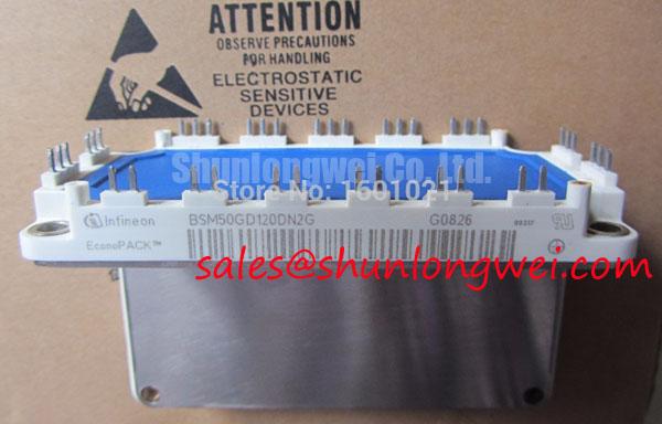
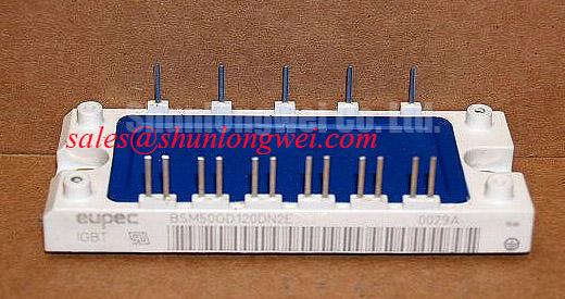
In heavy-duty variable frequency AC drive installations, output PWM voltage pulses with steep edge transitions (dv/dt exceeding 5 to 8 kV/µs) encounter an acoustic transmission line mismatch between the drive output cable and the motor stator winding. When cable lengths extend beyond critical distances, impedance discontinuities double the transient peak voltage at the motor terminals, subjecting phase-to-phase and turn-to-turn insulation to severe dielectric breakdown risks. For systems utilizing the BSM50GD120DN2E, which features a rated collector-emitter voltage of VCES = 1200V (Official Datasheet Specification) and a continuous collector current rating of IC = 72A at TC = 25°C (50A nominal class), managing these reflected wave transients requires properly sized dv/dt filters or passive line chokes directly at the inverter output terminals.
Field maintenance strategies dictate verifying the integrity of shielding terminations and measuring high-frequency common-mode leakage currents through the grounding grid. Incorporating symmetrical motor cables paired with ferrite core common-mode chokes attenuates peak terminal overvoltages below motor insulation threshold limits. System designers handling fast-switching dynamics can review baseline switching characterizations detailed in the Infineon TRENCHSTOP™ IGBT3 engineering documentation to ensure proper dv/dt margins under high switching frequency configurations.
Overvoltage Trip Prevention via Fast-Switching Ballast Chopper Topology
Rapid motor deceleration generates regenerative kinetic energy that pumps reverse current through the freewheeling diodes back into the DC link capacitor bank, rapidly elevating the intermediate bus voltage. To prevent high-voltage tripping or destructive overvoltage breakdown across the BSM50GD120DN2E power switches, a dedicated dynamic braking chopper circuit must engage seamlessly. Minimizing parasitic busbar stray inductance to values below 25 nH (Design Consideration for low-inductance busbars) is critical to prevent turn-off inductive overvoltage spikes, where the transient voltage equals the DC bus potential plus the inductive kick generated by rapid di/dt transitions.
⚠️ Field Alert: DC bus terminal torque calibration (standard industry practice of 2.5–3.5 N·m for M5 hardware) prevents contact loosening and high-resistance localized heating during repetitive regenerative cycles. Always install low-ESR polypropylene snubber film capacitors directly across the primary DC+ and DC- terminals to absorb high-frequency commutation energy. For detailed procedures on diagnosing snubber failure modes, capacitor degradation, and insulation testing during plant outages, refer to the Field Engineer’s Handbook.
Multi-Module Parallel Current Sharing & Positive Tempco Dynamic Balancing
The BSM50GD120DN2E exhibits a typical collector-emitter saturation voltage of VCE(sat) = 2.5V (3.1V maximum at IC = 50A, VGE = 15V, Tj = 25°C, Official Datasheet Specification) with a junction-to-case thermal resistance rated at RthJC ≤ 0.35 K/W per IGBT. At operating junction temperatures approaching the maximum allowable Tj max = 150°C, the device exhibits a positive temperature coefficient for VCE(sat), which acts as a self-regulating thermal balancing mechanism to prevent localized current hogging during continuous heavy-load operations.
⚠️ Maintenance Note: Periodically verify thermal interface grease condition. As silicone grease pump-out occurs over thermal cycles, the case-to-heatsink thermal resistance increases, causing junction temperature divergence across inverter phases. Clean heatsinks and reapply a uniform 50–100 µm thermal grease layer during scheduled preventative shutdowns.
When engineering high-capacity drives requiring expanded current handling, designers often evaluate dual-pack half-bridge topologies such as the FF150R12ME3G (rated at 150A / 1200V) to achieve modular scalability. Detailed layout guidelines for balancing parasitic loop inductances and driving parallel stages are outlined in the Infineon IGBT Paralleling Application Note.
Dynamic Gate Impedance Control for Robust Phase-Leg Dead-Time Operation
In high-power bridge topologies, high dv/dt transients generated during the turn-on of an opposing switch can couple charge through the Miller capacitance (Cres), inducing a spurious voltage spike on the gate of the un-driven switch. If this spike exceeds the typical gate-emitter threshold of VGE(th) = 5.5V (Official Datasheet Specification at IC = 2mA), shoot-through cross-conduction occurs across the DC bus, causing rapid thermal failure.
Preventative driver design requires applying a stable negative turn-off bias (typically -5V to -15V) or utilizing an active Miller clamp circuit that short-circuits the gate-emitter loop when the device is commanded off. Setting hardware interlocking dead-times (typically 1.5 to 2.5 µs as a Typical Starting Point for bench tuning) ensures complete carrier recombination in the freewheeling diodes and collector channel before the complementary IGBT is energized, eliminating cross-conduction risks during extreme factory temperature fluctuations.