

Content last revised on September 13, 2026
Benchtop Waveform Tuning: Mitigating Stress via Symmetrical Busbar Geometry for FZ2400R17KF4
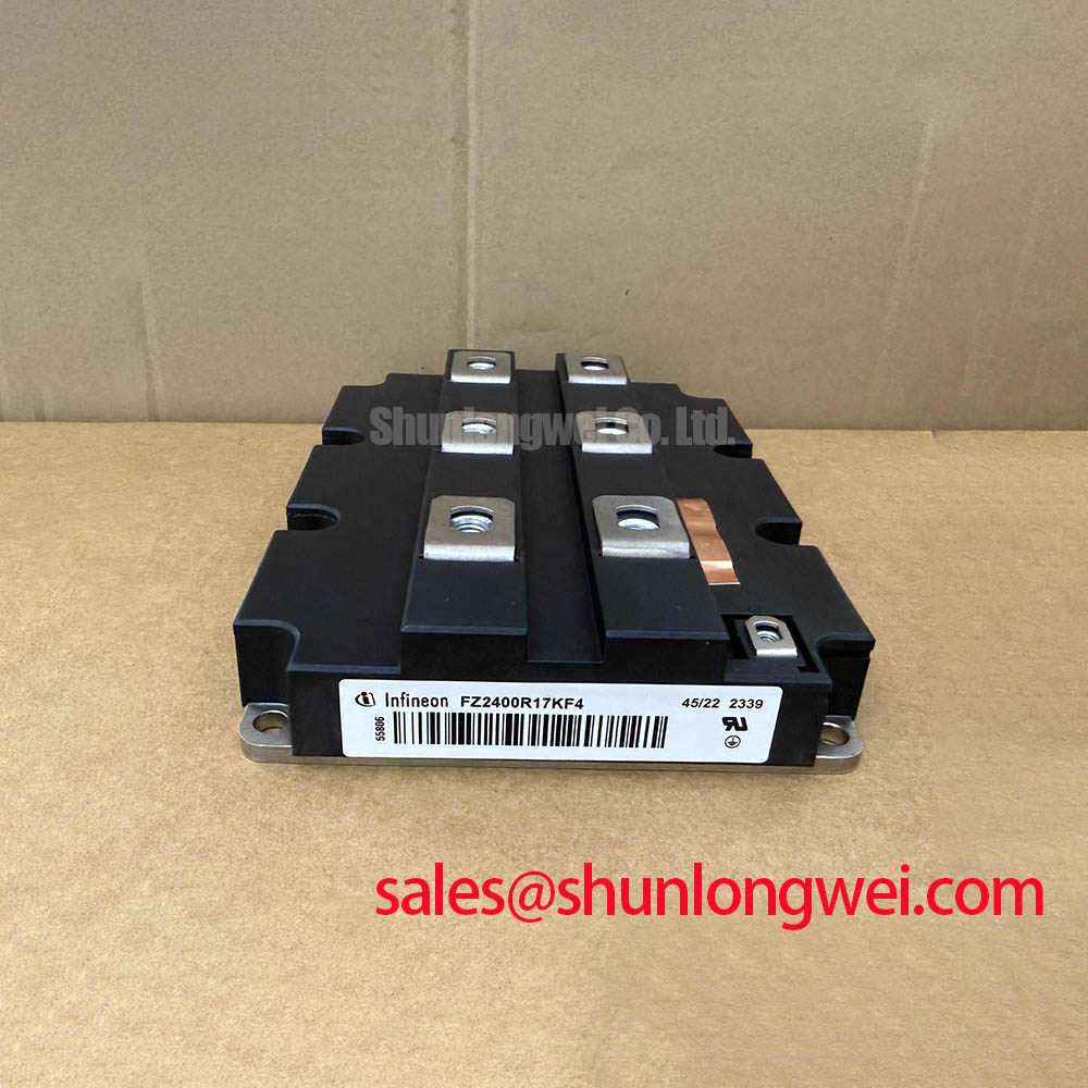
Begin service evaluation by isolating the DC link, inspecting the module terminals and housing, and confirming the nameplate boundary before applying any test voltage. The Infineon FZ2400R17KF4 is a single-switch IGBT module with an official VCES rating of 1700 V, an official continuous DC collector current rating of 2400 A, and an official repetitive peak collector current rating of 4800 A for 1 ms. These values identify the electrical class of the device, but they do not replace the switching, thermal, and protection limits of the complete converter.
For a multi-megawatt offshore or onshore wind turbine full-scale converter, begin waveform work at a controlled operating point and compare collector-emitter voltage, gate-emitter voltage, collector current, and freewheel diode recovery on the same time base. A symmetrical busbar path helps make the commutation environment repeatable. The positive temperature coefficient commonly associated with IGBT saturation voltage can support static current sharing between parallel semiconductor paths, but dynamic sharing is strongly influenced by stray inductance, gate-loop impedance, driver timing, and the physical position of the current sensors.
This is a Design Consideration, not an FZ2400R17KF4 factory guarantee: keep the high-current commutation path compact and geometrically balanced, with the forward and return conductors arranged so that their magnetic fields partially cancel. The switching loop should be separated from sensitive gate-drive and measurement wiring. Designers should verify the actual clearance and creepage requirements against the working voltage, pollution environment, insulation system, and applicable equipment standard rather than applying a generic spacing value.
The freewheel diode path deserves separate attention. Reverse-recovery softness factor S is not provided in the supplied factory parameter set, so it should be taken from the applicable device documentation or measured on the completed commutation network. A softer recovery characteristic can reduce the abrupt current transfer that excites common-mode voltage and radiated EMI, but the result depends on DC-link inductance, loop geometry, gate resistance, junction temperature, and switching speed. Use a calibrated current probe and a short, properly compensated voltage probe when comparing a known-good converter leg with a service replacement.
When a waveform shows excessive ringing, do not assign the condition to the IGBT alone. Inspect laminated busbar alignment, terminal flatness, clamping pressure, probe ground inductance, snubber connections, and the physical route of the diode return path. If a replacement module is being evaluated, the FF45017ME4 may be reviewed as a separate device candidate, but voltage class, current capability, topology, mechanical interfaces, thermal impedance, gate behavior, and protection coordination must be verified independently before any substitution.
Assembly Integrity and Layout Architecture: Applying Reliability Data Carefully to FZ2400R17KF4
The official insulation test voltage for the FZ2400R17KF4 is VISOL = 4.0 kV RMS. This rating is an insulation test specification, not permission to expose the installed module to arbitrary repetitive common-mode stress. Before energizing a repaired converter, verify terminal identity from the original module documentation and the equipment schematic. Confirm that collector, emitter, gate, auxiliary return, and any designated sensing terminals are connected according to the specified topology; do not infer a pin function from physical similarity alone.
Mechanical assembly should maintain a flat, clean contact interface between the module and its thermal path. Remove conductive debris, inspect the busbar contact surfaces, and check that fasteners apply even pressure without distorting the terminal stack. Any mounting torque used in production should come from the module documentation and the converter assembly specification. Vibration-resistant fastening is a system design matter: the engineer should validate joint retention, busbar flexure, insulation support, and thermal cycling under the actual enclosure conditions.
Altitude and terrestrial neutron exposure require disciplined qualification rather than a guessed failure-rate calculation. At elevations above 2000 m, reduced air density can affect external insulation performance and cooling behavior, while neutron-induced single-event effects depend on semiconductor technology, applied voltage, switching state, shielding, mission profile, and statistical evidence. No FIT rate, SEB probability, or operating-life figure should be assigned to this product without an authoritative source such as a manufacturer reliability document, a recognized qualification report, or a documented system-level study.
The practical response is to establish the converter’s maximum DC-link voltage, transient overshoot, insulation environment, cooling capability, and altitude envelope, then compare those conditions with the current device documentation and the system safety analysis. The available DC-bus headroom should be determined from measured switching peaks and the approved design margin, not from the 1700 V label alone. A double-pulse test, temperature sweep, and insulation verification can reveal whether the installed layout behaves as expected.
For system context, the Infineon PrimePACK™ module family provides useful manufacturer-level reference material on industrial IGBT module integration. It should be treated as technical background and not as a substitute for the exact FZ2400R17KF4 documentation. Likewise, system integrators evaluating a front-end or complementary power stage can review FZ3600R12HP4, while independently checking its voltage class, switching role, terminals, and protection requirements.
Preventing Spurious Faults: Active Miller Clamp Implementation Guidelines for FZ2400R17KF4
High collector-voltage slew rates can couple through the effective reverse-transfer capacitance and raise the voltage of a nominally inactive gate. The relevant capacitance and charge values for this behavior are not included in the supplied factory parameter list, so the driver must be developed from the applicable datasheet curves and verified on the actual module, busbar, and gate circuit. The design objective is to keep the inactive gate firmly controlled during the opposing switch transition without adding damaging loop inductance or excessive driver dissipation.
An active Miller clamp is a Design Consideration for this task. It normally provides a low-impedance discharge path after the gate signal has crossed the driver’s turn-off threshold. Its effectiveness depends on clamp placement, driver propagation delay, common-emitter voltage movement, gate resistor arrangement, and the distance between the driver return and the module’s designated gate-return terminal. The system designer should determine whether a negative gate bias is required from the module’s gate-emitter limits, driver capability, fault behavior, and insulation architecture. The specific bias value must come from the approved design, not from a generic recommendation.
Keep the active clamp connection close to the gate and its corresponding emitter reference. Avoid routing the clamp return through the high-current emitter path, because shared impedance can convert di/dt into an apparent gate-drive disturbance. A split gate resistor arrangement can help separate turn-on and turn-off behavior, but its values and pulse ratings remain system-determined. During commissioning, observe the inactive gate directly at the module terminals and compare it with the driver output at the board connector. A discrepancy between these locations may indicate parasitic coupling or reference movement rather than a defective driver.
Cross-conduction troubleshooting should proceed by checking gate timing, dead-time behavior, driver supply stability, clamp activation, isolation-channel delay, and the collector-emitter voltage of both switches. Do not interpret a single fault waveform as proof of one failed component. Verify the signal path with a differential probe, inspect the gate resistor and clamp components for pulse damage, and repeat the test at controlled current and voltage conditions. The Infineon HybridPACK™ Drive reference material can help explain modern gate-drive and power-loop principles, although its application data is not a specification for this industrial module.
Protection coordination also extends beyond the gate driver. A semiconductor fast fuse must be selected by comparing its available clearing characteristic and I²t behavior with the converter’s fault energy, DC-link capacitance, conductor impedance, and the module’s short-circuit withstand information from the approved documentation. The fuse cannot be treated as a universal guarantee against a dead short. The complete protection chain should be tested for detection delay, interruption behavior, thermal stress, and enclosure fault containment.
Gate Drive Loop Geometry: Separating Auxiliary Return Paths on FZ2400R17KF4
When the module documentation identifies a separate auxiliary emitter or sensing return, use that terminal only for the gate-drive reference and measurement circuit. The main emitter conductor carries substantial switching current and can develop a transient voltage across its parasitic inductance. If the driver shares that path, the controller may see an artificial gate voltage shift, producing oscillation, delayed turn-off, uneven switching, or nuisance protection trips.
This is an Engineering Recommendation: route the auxiliary return independently from the main power emitter trace, keep the gate and return pair physically close, and minimize the enclosed area of the gate-drive loop. The power commutation loop and the gate loop should cross only where the layout requires it, preferably with controlled geometry and appropriate insulation. Designers should validate the final arrangement through double-pulse testing, checking gate overshoot, turn-on and turn-off transitions, collector-emitter overshoot, and current sharing under the intended temperature range.
Do not assume that a visually short copper route has low effective inductance. Via transitions, connector pins, laminated busbar joints, mounting interfaces, and probe attachments can all alter the measured waveform. During field diagnosis, compare the gate signal at the driver output with the signal directly across the module gate and its specified return. Inspect for loose auxiliary terminals, cracked solder joints, oxidized contact surfaces, and damaged gate resistors. A difference between the driver reference and the module reference may indicate mutual coupling or an assembly problem that requires layout correction.
The FZ2400R17KF4’s 1700 V VCES and 2400 A continuous DC collector current ratings must be evaluated together with switching frequency, junction temperature, cooling resistance, pulse profile, and converter control strategy. The 4800 A, 1 ms ICRM value is an official repetitive peak-current specification, not a general-purpose short-circuit or overload allowance. Thermal measurements should be taken at the defined reference points, and the results should be compared with the authorized thermal data for the exact device and assembly.
Safety Interlock Note: Fully discharge and verify the DC link before touching gate, auxiliary, or power terminals, even when the converter control system reports an inactive state.
For broader application context covering IGBT use in renewable-energy and heavy-industry power conversion, engineers can consult the Industrial Applications resource. The final integration decision should remain tied to the original converter drawings, verified terminal mapping, measured switching waveforms, insulation coordination, cooling design, and the exact manufacturer documentation for the FZ2400R17KF4.