


Content last revised on September 12, 2026
CM1000DUC-34SA Circuit Protection and Reliability in Four-Quadrant PCS Power Flow
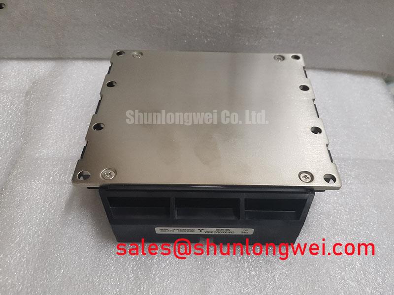
In a utility-scale centralized battery energy storage PCS, the power stage must manage energy transfer in both directions between the battery-side DC system and the inverter link. The CM1000DUC-34SA may be evaluated for such a high-current conversion position when its electrical topology, cooling arrangement, gate-drive requirements, and protection coordination match the original equipment design. Its official ratings are VCES = 1700 V and IC = 1000 A; these values do not by themselves establish an allowable operating point for every switching condition.
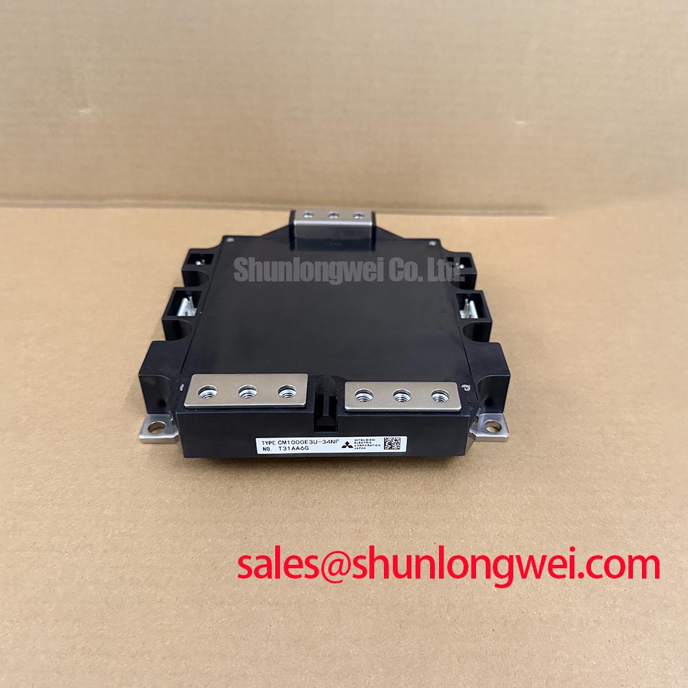
During incoming inspection, compare the device marking with the purchase specification, then verify the intended collector, emitter, and gate connections against the original circuit drawing. A resistance check between power terminals can help identify an obvious shorted condition, but a single multimeter reading is not a complete semiconductor qualification test. The diode-test function should be used only with the device isolated from the gate driver and DC-link capacitors. Record the polarity, displayed forward voltage, and measurement direction for comparison with a known-good unit of the same configuration. Do not infer a precise internal fault threshold from an unpowered meter result.
Four-quadrant operation increases the importance of coordinated switching transitions. During battery charging, discharging, regeneration, and reactive-power control, the control system can expose the power module to repeated current reversals and changing thermal loading. This is a Design Consideration rather than a device-specific life guarantee. Engineers should examine junction-temperature estimates, case-temperature measurements, cooling-plate flatness, airflow or coolant conditions, and the actual current waveform during representative peak-shaving cycles.
For the AC side, the rectifier and modulation strategy should be reviewed together. Phase-controlled rectification can increase low-order and higher-order current harmonics when the conduction angle is narrow or the grid-side impedance is significant. Harmonic filtering, active front-end control, and the selected firing or switching strategy remain system-level decisions. The CM1000DUC-34SA rating does not certify the complete PCS for grid harmonic compliance or EMC performance. Applicable project requirements should be checked against the relevant grid code and the final equipment test report.
When comparing a replacement in the same equipment family, engineers may place FF45017ME4 beside the original bill of materials for a documented electrical, mechanical, and drive-interface comparison. This is an evaluation reference, not a universal substitution recommendation. Check voltage class, current conditions, mounting geometry, terminal configuration, thermal path, and protection timing before approving any alternate.
Field Diagnostics and Commissioning for Gate-Controlled CM1000DUC-34SA Topologies
Gate commissioning should begin with the driver disconnected from the power bus. Confirm the gate-emitter reference at the module connector, check continuity of the driver return path, and inspect whether power and gate wiring have been separated as required by the original design. A Kelvin emitter or auxiliary emitter connection must not be assumed from the model name alone; the system integrator should verify the terminal definition from the applicable drawing before routing a separate feedback conductor.
High common-mode voltage during switching can couple into the opposing gate circuit and create an unwanted turn-on condition. An active Miller clamp is a Design Consideration for reducing this risk when the selected driver supports it. The clamp path should be physically short and referenced to the correct emitter return. Any negative gate bias, including the commonly discussed range of minus five to minus fifteen volts, is an application-dependent setting and must not be treated as an official CM1000DUC-34SA parameter without a supporting datasheet or application note. The driver manufacturer’s absolute maximum gate-emitter limits must control the final setting.
Dead-time protection also requires measurement rather than assumption. Observe both gate-emitter waveforms and the corresponding collector-emitter transitions with probes suitable for the switching environment. A dead-time interval that is too short can increase cross-conduction risk, while excessive dead time can raise switching loss and distort the commanded waveform. The correct value depends on driver propagation delay, temperature, load current, device variation, and the complete gate loop. Verify the result under cold and warmed operating conditions.
The thermal interface should be applied consistently across the approved cooling surface, with the interface material and application method taken from the equipment service documentation. A nominal 50 to 80 micrometre layer is a general integration reference only, not an official parameter for this module. If the mounting system uses multiple screws, tighten them in a cross-pattern sequence appropriate to the heatsink and hardware specification so that the baseplate is not locally distorted. Bench Tip: keep the module isolated from charged capacitors, use ESD protection, and compare cold-state diode-test readings with a known-good reference before connecting the gate driver.
In a PCS containing a separate front-end rectifier or related conversion stage, the service engineer can document the interaction between the IGBT gate supply, DC-link precharge, and rectifier section. The CM50DY-28H can be reviewed as a related topology component during that comparison. Its presence does not define the internal circuit of the CM1000DUC-34SA, so the actual schematic and terminal schedule remain the controlling references.
Symmetrical Busbar Geometry and High-Current Sharing Checks
At 1000 A rated current, busbar geometry and connection resistance deserve inspection before any high-power test. Keep parallel current paths physically similar where the circuit uses multiple modules or parallel switching positions. Differences in conductor length, contact pressure, stray inductance, and gate-loop routing can produce unequal current during fast transitions even when the nominal semiconductor ratings appear identical.
A positive temperature coefficient of on-state voltage can support static current sharing under suitable parallel operating conditions, because a warmer device may naturally carry less incremental current. This is a general semiconductor Design Consideration, not a guarantee that dynamic sharing will be balanced. During commissioning, use synchronized voltage and current measurements to compare branches while changing load gradually. A branch that shows unusual current imbalance should be investigated through busbar resistance, terminal seating, gate timing, sensor calibration, and thermal contact rather than assigned to one cause without evidence.
Symmetrical gate wiring is particularly important when several switching positions share a DC link. Place the driver reference conductors according to the approved schematic and avoid routing a high-current commutation path beside a sensitive gate-return path. Minimize parasitic loop inductance to suppress turn-off overshoot, then verify peak collector-emitter voltage against the DC-link voltage during switching tests. The required clearance and creepage distances are system insulation-design values; they must be selected from the working voltage, pollution environment, altitude, material group, and applicable safety standard rather than inferred from the module’s 1700 V rating.
For field troubleshooting, first capture the DC-link voltage, gate-emitter waveform, collector-emitter waveform, and case temperature under a controlled test condition. If one branch turns off earlier or exhibits a larger voltage spike, compare the complete signal path with the corresponding known-good branch. Inspect laminated busbar alignment, fastening surfaces, gate resistor population, auxiliary emitter routing, and current-sensor polarity. These checks are more reliable than diagnosing a module from a single audible event or a static resistance value.
Transient Thermal Impedance and Electrical Design Verification
Pulsed overload analysis should start with the actual load profile rather than the 1000 A nameplate value. Record pulse duration, repetition pattern, current direction, switching state, case-temperature boundary, and cooling-system response. A transient thermal model can then represent junction-to-case behavior with several RC sections, but the model coefficients must come from the applicable manufacturer thermal data or a validated laboratory characterization. They should not be invented from the module’s voltage and current ratings.
For a short overload, the instantaneous junction temperature may not track the case temperature. The engineer should therefore combine the measured case temperature with the manufacturer’s transient thermal impedance curve, semiconductor conduction loss, switching loss, and the real gate-drive waveform. Peak junction-temperature margin is calculated only after these inputs are established. If the original specification does not provide the required transient curve, the safe engineering action is to obtain the data or reduce the test envelope while monitoring the device, rather than assign an assumed thermal constant.
Protection must address both electrical and thermal stress. A desaturation or collector-emitter monitoring circuit may be considered for short-circuit detection, with a controlled soft turn-off strategy used where the driver and module documentation support it. The correct blanking interval, fault threshold, gate discharge path, and short-circuit response must be determined from validated switching tests. SCSOA behavior and short-circuit withstand time are not included in the supplied official parameters for this page, so they should be confirmed before a protection circuit is approved.
Do not combine a pulsed overload test with an unverified cooling interface. Recheck mounting flatness, thermal compound coverage, cooling-plate temperature uniformity, and the isolation arrangement after the test. For wider background on high-power semiconductor technology and design tradeoffs, engineers can consult Wide Bandgap Revolution, while device-family information should be checked through Mitsubishi Electric Power Semiconductors and High-Power Modules and Mitsubishi Electric Global Semiconductor Device Technologies.
Before release to service, document the measured gate polarity, isolated diode-test observations, DC-link precharge behavior, protection response, current sharing, case temperature, and switching overshoot. The final PCS acceptance decision should be based on the equipment schematic, verified Mitsubishi Electric documentation, applicable safety requirements, and measured operating margins.