Content last revised on September 12, 2026
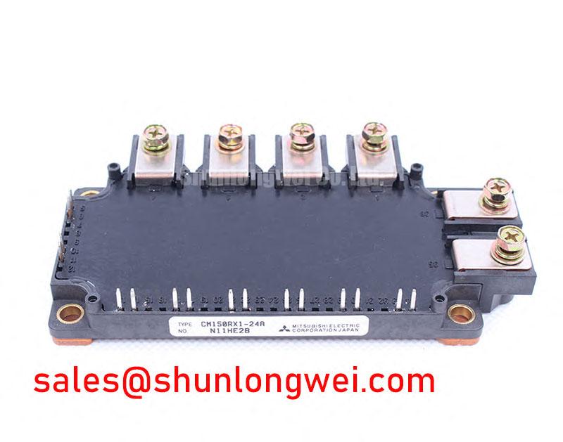
| Manufacturer | Mitsubishi Electric |
|---|---|
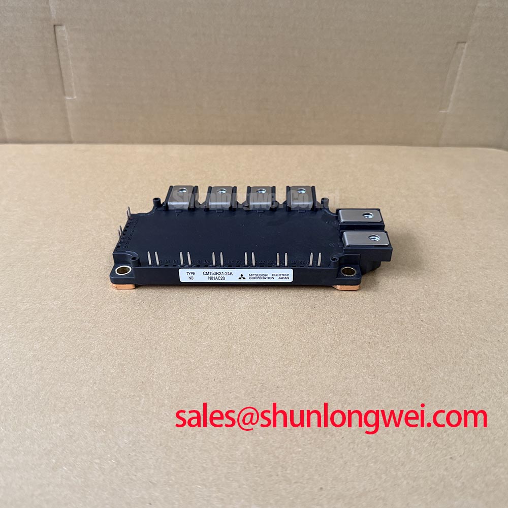
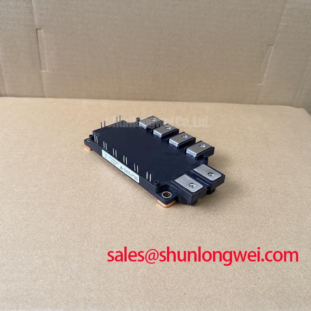
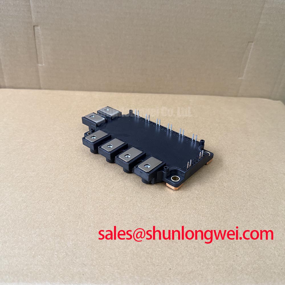
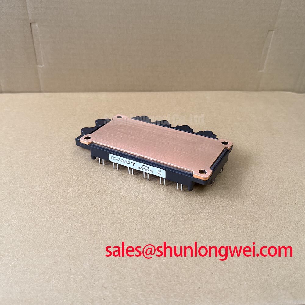
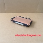
| Model | CM150RX1-24A |
| Product category | IGBT Module |
| Rated voltage | 1200.0 V |
| Rated current | 150.0 A |
| Package | Module |
CM150RX1-24A Operational Boundaries: Evaluating DC-Link Capacitance Bank Layout and Low-ES Limits
Probe the DC-link positive and negative rails at the module terminals with a differential oscilloscope connection, then compare the measured turn-off overshoot with the 1200.0 V voltage rating of the Mitsubishi Electric CM150RX1-24A. This measurement should be made at the switching terminals rather than several centimetres away on the capacitor bank, because busbar inductance and probe-loop inductance can conceal the actual stress seen by the power module.
The official electrical identity supplied for this device is a 1200.0 V, 150.0 A IGBT module in a module package. These are product ratings, not a complete operating prescription for a variable frequency drive. The actual permissible switching voltage, current, pulse duration, temperature, and repetition rate remain dependent on the electrical and thermal conditions defined by the applicable technical documentation and the finished converter.
During a hard commutation event, the switching-node peak is influenced by the DC-link voltage and the product of stray inductance and current change rate. This relationship is useful as an Engineering Calculation when interpreting a waveform, but it does not establish a universal layout limit for this model. Designers should minimise the high-current commutation loop, place the low-impedance capacitor bank close to the switching path, and verify the resulting peak voltage during double-pulse or equivalent switching tests.
A practical inspection begins with the capacitor bank, laminated busbar, terminal interfaces, and snubber connection. Look for uneven current paths, long narrow copper sections, loose mechanical joints, and capacitor groups connected at visibly different distances from the module. Low equivalent series resistance and low equivalent series inductance are Design Considerations because they influence ripple current circulation and transient voltage response. The required capacitance and damping network must be determined from the converter topology, operating point, switching waveform, and thermal measurements.
For a heavy-duty variable frequency AC motor drive, the DC-link bank also interacts with rectifier ripple, regenerative energy, braking events, and motor-cable capacitance. A smooth-looking rail under line-frequency operation does not prove that the switching loop is adequately controlled. Capture the bus voltage at light load, rated-load conditions, acceleration, deceleration, and fault interruption where the test procedure permits. Compare the traces from each phase leg to identify asymmetry rather than assigning one observed symptom to a single cause.
RC snubbers can reduce high-frequency ringing when their impedance, placement, pulse-energy capability, and damping behaviour match the switching network. Their values should be selected from measured ringing frequency, energy evaluation, and device operating conditions. Installing a generic capacitor directly across the main terminals without checking pulse current and dissipation can introduce a different resonant path. Any clamp or snubber decision is therefore an Engineering Recommendation requiring bench validation.
When a replacement evaluation involves a related voltage or current class, engineers may also review CM150DY-12NFA as a separately specified comparison candidate. Electrical pinout, switching characteristics, thermal interface, gate-drive requirements, and mechanical fit must be compared before any substitution is considered.
Benchtop Waveform Tuning: Mitigating Stress via Dynamic Power Loss Dissipation and Multi-R on CM150RX1-24A
Connect voltage and current probes at the same switching event, calculate instantaneous device power from the captured waveforms, and correlate the pulse energy with case temperature while tuning the CM150RX1-24A on a controlled bench. This method separates conduction loss, turn-on loss, turn-off loss, and transient ringing more reliably than judging temperature from a heatsink surface alone.
The module carries an official current rating of 150.0 A, but a current rating by itself does not specify permissible overload duration or switching frequency. The operating point must be checked against junction temperature, case temperature, cooling performance, duty cycle, gate-drive behaviour, and the relevant manufacturer curves. A short high-current pulse and a continuous high-current condition place different demands on the thermal path.
Transient thermal evaluation should use the applicable junction-to-case thermal impedance information rather than treating the thermal resistance as a fixed number under every pulse condition. A multi-RC representation is an Engineering Calculation used to approximate how heat moves from the semiconductor junction into the case over time. The calculated peak junction temperature should then be checked against the documented rating and validated with measured case temperature and realistic pulse repetition.
For a variable frequency AC motor drive, line-frequency ripple from the rectifier can modulate the DC-link voltage and change both conduction and switching loss. Capture the waveform over the complete electrical cycle when examining phase-angle conduction, rectifier interaction, or braking transitions. If a controlled rectifier or thyristor stage is present upstream, verify its gate trigger conditions, including the documented gate-trigger current and gate-trigger voltage for that separate device. Do not infer IGT or VGT values for the Mitsubishi Electric IGBT module from a thyristor circuit.
Pulse-train triggering can improve repeatability in a thyristor gate circuit when the selected trigger method is compatible with the thyristor data and isolation arrangement. That control decision belongs to the rectifier stage, while the IGBT gate loop requires its own voltage, current, timing, Miller-control, and protection verification. The system integrator should examine dead-time coordination so that opposing devices are not commanded into simultaneous conduction during a transition.
Multi-R gate networks can be used as a Design Consideration when turn-on and turn-off behaviour need independent damping or when separate switching paths require waveform balancing. The starting values should be selected from the actual gate-charge behaviour, driver output capability, common-emitter inductance, and measured VGE waveform. A resistor that appears suitable at low current may produce excessive delay, ringing, or uneven dynamic sharing at the intended operating point.
The gate-drive supply and isolation arrangement should be checked alongside the power waveform. Confirm the return path, driver saturation behaviour, desaturation or overcurrent response, and fault-reset sequence with the module disconnected or under a controlled low-energy test condition. The exact protection threshold and response time are system parameters unless explicitly specified for the device and driver combination.
For related front-end topology evaluation, the CM150MXUD-24T can be reviewed as a separately specified device within a broader converter architecture. Its presence in a system does not establish electrical compatibility with the CM150RX1-24A; voltage class, current path, control method, pin arrangement, and thermal conditions must be assessed independently.
Benchtop Waveform Tuning: Mitigating Stress via Auxiliary Emitter Return Trace Separation on CM150RX1-24A
Measure the gate-to-emitter voltage directly at the module control terminals while simultaneously observing the main emitter current path; any difference between the driver reference and the local emitter reference should be treated as a layout investigation point. The purpose is to determine whether the gate loop is being disturbed by voltage developed in a shared high-current return conductor.
A gate driver responds to the voltage between its gate output and emitter reference, not to a remote ground point that appears electrically common on a schematic. When the auxiliary emitter return shares copper with a rapidly changing power current, mutual coupling and common impedance can alter the apparent VGE waveform. This may appear as unwanted gate oscillation, delayed turn-off, false protection response, or inconsistent switching between phase legs. Confirm the condition with a short probe connection and a known-good measurement arrangement.
Keep the gate command path and its emitter return physically close as a matched loop, while keeping that reference path separate from the main high-current emitter route until the intended connection point. This is a Design Consideration rather than an official package parameter. The final geometry depends on terminal arrangement, gate-driver isolation, busbar construction, creepage requirements, service access, and the complete power-loop layout.
Inspect the control connector, solder joints, terminal hardware, and any intermediate interface board for unintended shared returns. Continuity at zero power does not demonstrate acceptable dynamic behaviour. Use an oscilloscope to compare gate voltage, collector-emitter voltage, and current at the same time. A ringing gate waveform may also be influenced by driver output impedance, gate resistance, Miller coupling, supply decoupling, or measurement technique, so the investigation should preserve the complete signal path.
Dead-time should be evaluated from actual turn-off and turn-on waveforms rather than copied from an unrelated module. The appropriate interval is system-determined and must account for driver propagation mismatch, temperature, current, DC-link voltage, and the switching characteristics documented for the selected device. Excessive dead-time can increase diode conduction and distortion, while insufficient dead-time can create cross-conduction risk.
Symmetry matters when multiple phase legs operate under comparable conditions. Route corresponding gate loops with comparable geometry, avoid placing sensitive gate traces alongside high dv/dt nodes, and verify the result at the highest intended switching stress. Designers should also confirm that the isolated driver supply remains stable during fault events and that the control reference does not lift relative to the power-stage reference.
Pro Tip: Use a symmetric planar commutation layout and verify turn-off voltage margin with a calibrated differential probe during switching tests instead of relying on schematic-level net names.
The Mitsubishi Electric NX-Series IGBT Module reference provides useful manufacturer-level context for power-module evaluation, while the Mitsubishi Electric SiC power device information helps distinguish IGBT gate-drive assumptions from those used with other semiconductor technologies. Neither reference should be used to transfer unverified ratings to the CM150RX1-24A.
CM150RX1-24A Thermal-Electrical Optimization: Derating Guidelines and Mismatched Parameter Practical Tuning
Compare each phase leg’s collector-emitter voltage, current waveform, gate voltage, and case temperature under the same load condition before adjusting any control or cooling parameter. This side-by-side test helps identify mismatched wiring, unequal thermal contact, driver timing variation, or external impedance differences around the CM150RX1-24A.
The specified 1200.0 V voltage rating and 150.0 A current rating define key product boundaries, but they do not remove the need for application derating. Designers should evaluate the highest DC-link voltage, switching overshoot, peak phase current, average current, ambient temperature, cooling path, overload profile, and fault interruption behaviour together. Derating is a Design Consideration established by the system verification plan and the applicable technical data.
Parallel semiconductor paths can benefit from the positive temperature coefficient of IGBT on-state voltage in steady-state current sharing, but this effect should not be treated as a guarantee of dynamic balance. During fast transitions, gate-loop inductance, driver propagation mismatch, emitter coupling, busbar geometry, and device parameter spread can dominate. Match the physical gate-loop arrangement and measure current sharing during turn-on, turn-off, acceleration, deceleration, and regenerative operation.
Thermal interface preparation deserves the same attention as electrical layout. Ensure that the mounting surface is clean, flat, and mechanically stable, and apply the selected interface material according to its manufacturer’s process guidance. The heatsink, airflow or coolant path, clamping structure, and case-temperature measurement point should be assessed as one thermal system. Do not use a heatsink temperature reading as a direct substitute for junction temperature.
For bidirectional DC-DC battery charging and discharging systems, alternating power flow can create thermal cycling even when the average electrical power appears moderate. Evaluate the junction-to-case thermal response over the complete charge and discharge sequence, including current reversal and control transitions. The resulting lifetime assessment requires qualified mission-profile data and reliability methodology; unsupported field-life or failure-rate figures should not be assigned to this module.
When waveform mismatch remains after the gate-return and busbar paths have been checked, compare driver supply voltage, gate resistance, protection timing, current-sensor delay, and PWM command timing. Change one controlled variable at a time and retain the original waveform for comparison. This approach avoids attributing every thermal difference to semiconductor variation when the cause may be external to the module.
System topology also affects the interpretation of ringing, conduction angle, and regenerative current. Engineers assessing resonant or semi-resonant appliance converters can consult Resonant Topologies in Home Appliances for topology-level background, while the CM150RX1-24A must continue to be evaluated against its own documented electrical and mechanical requirements.
Use the measured operating envelope to decide whether additional damping, revised cooling, altered switching timing, or a different module class merits investigation. Any alternative device requires an independent comparison of rating, terminal configuration, gate behaviour, thermal data, isolation requirements, mechanical fit, and protection coordination before the equipment is returned to service.