

Content last revised on October 5, 2026
Benchtop Waveform Tuning for Dynamic Power Loss Evaluation
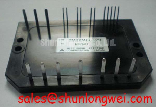
| Manufacturer | Mitsubishi Electric |
| Model | CM20MDL-12H |
| Product Category | IGBT Module |
| Rated Voltage | 600.0 V |
| Rated Current | 20.0 A |
| Package | Module |
Probe the gate and power terminals with the inverter disabled, then compare cold-state terminal behavior with a known-good signal path before applying switching pulses to the CM20MDL-12H. The published device ratings are 600.0 V and 20.0 A; these values define the component identification boundary, not an automatic operating point for every converter.
For a compact industrial inverter or high-speed CNC spindle drive, observe collector-emitter voltage, gate-emitter voltage, current rise, turn-off overshoot, and ringing during a controlled bench test. Dynamic power loss depends on switching frequency, load current, gate-drive behavior, commutation path, DC-link impedance, and thermal conditions. The transient thermal response should therefore be evaluated through the system’s applicable Zth model or validated thermal test data rather than inferred from the package label.
A multi-RC thermal network can be used as an Engineering Calculation method when the required thermal impedance data is available from the applicable technical documentation. Calculate the pulse temperature rise from the measured loss waveform and the relevant transient thermal impedance, then compare the resulting junction estimate with the permitted device and system limits. Without verified Zth data, use thermocouple measurements, case temperature tracking, and repeated pulse testing to identify whether the observed waveform is thermally sustainable.
When switching stress appears excessive, inspect the commutation loop for unnecessary inductance, verify the DC-link capacitor connection, and check whether the gate loop shares a noisy return path with the power loop. A MOV or other overvoltage absorption network may be evaluated around the converter according to the DC-link voltage, surge energy, repetition rate, and clamping characteristics selected by the system designer. The protection network must be validated against the actual switching waveform rather than specified from the IGBT voltage rating alone.
For welding inverter and related high-current converter references, engineers can review Welding Power Supply High-Current Inverters. Current feedback should also be checked at the same physical location used by the control loop; LEM High-Precision Current Transducers for Power Inverters provides a relevant reference for power inverter current measurement.
Assembly Integrity and Gate Isolation Architecture
Measure gate-to-emitter resistance and diode-mode behavior at the external terminals with the module isolated from the driver board, recording the cold-state readings before investigating an unexpected trigger or missing pulse. These checks can reveal a wiring error, contamination path, or abnormal terminal impedance, but they do not replace a controlled dynamic test.
An optocoupler and a digital coreless transformer represent different gate-drive isolation approaches. The correct choice depends on isolation coordination, propagation delay, common-mode transient behavior, drive-current capability, fault handling, and the switching environment. Specific isolation voltage and CMTI values must be taken from the selected driver’s documentation; they are not established by the CM20MDL-12H rating data provided here.
Keep the gate-drive return physically associated with the corresponding emitter connection and minimize the area of the switching gate loop. During troubleshooting, place the oscilloscope reference carefully and use suitable differential probing so that a measurement loop does not create an apparent gate pulse. If a false turn-on event is suspected, compare the gate waveform with the collector-emitter transition and inspect the driver supply for disturbance.
When more than one power module is used in a system, static current sharing should be treated as a Design Consideration. Device parameter spread, thermal coupling, busbar resistance, gate timing, and temperature-dependent conduction characteristics all influence the result. Designers should establish sharing through matched electrical paths and measured current distribution rather than assuming that a positive temperature coefficient will provide sufficient balance for every operating condition.
For a hardware replacement evaluation, compare terminal arrangement, electrical ratings, mechanical interface, gate-drive requirements, and protection coordination before considering the CM30TF-12E as a separate candidate. The linked part should be assessed on its own documentation and system compatibility, not treated as an automatic substitute.
Baseplate Thermal Interface and Fastening Control
Inspect the mounting surface for burrs, contamination, uneven contact, and visible curvature before applying thermal interface material beneath the CM20MDL-12H. A poor interface can increase case temperature even when the electrical waveform appears acceptable.
Thermal grease thickness is a system assembly variable governed by the module contact surface, heatsink flatness, compound rheology, mounting pressure, and the thermal resistance target. Use the compound supplier’s application method and the module manufacturer’s mechanical instructions; do not treat a generic thickness value as an official parameter for this model. The objective is a continuous interface with controlled displacement and minimal trapped air, not a visually heavy layer of paste.
For double-sided cooling or pressure-mounted assemblies, verify that the pressure mechanism distributes load evenly across the permitted contact area. Disc springs, clamps, or sequential fasteners should be calibrated according to the mechanical design and validated with the applicable force or torque specification. A mounting torque copied from another package can distort the baseplate, damage the substrate, or create uneven thermal contact.
After installation, inspect the spread pattern of the thermal interface material on a qualification sample and record heatsink flatness, fastening order, and measured case temperature. If a thermal hotspot remains, compare both sides of the interface, check the sensor position, and repeat the test under the same load waveform. This separates interface variation from switching loss and cooling-system limitations.
Bench Tip: Keep the module and test leads within an ESD-controlled workspace, and compare cold-state terminal measurements before connecting the gate driver or DC-link source.
Symmetrical Busbar Geometry and Protection Coordination
Check each power path for equal conductor length, similar contact pressure, and consistent terminal seating when a current imbalance appears during a high-current pulse test. A symmetrical busbar layout reduces differences in stray inductance and resistance, but the final balance must be verified with isolated current measurements and synchronized voltage probes.
Gate-loop wiring should follow the same physical symmetry as the power path where parallel switching devices are used. Keep gate conductors away from high dv/dt nodes, avoid shared return impedance, and verify turn-on and turn-off timing at every driver connection. The system designer should determine acceptable peak voltage margins against the DC-link voltage during switching tests; the 600.0 V device rating does not define the complete transient margin of the assembled inverter.
Fast semiconductor fuses may be coordinated with the converter by comparing their clearing behavior and I²t capability with the module’s short-circuit withstand and fault-clearing requirements. Those values must come from the applicable manufacturer documentation and the tested protection circuit. A fuse selected only by nominal current can fail to protect the semiconductor during a severe fault, while an unsuitable device may interrupt normal current transients unnecessarily.
Use the same measurement reference when evaluating a MOV, DC-link clamp, snubber, or active protection circuit. Record clamping voltage, pulse repetition, wiring inductance, and energy path during the test. The broader application context can be reviewed through Industrial Applications, while the final protection network remains dependent on the converter topology and verified test results.
For a compact CNC spindle drive, investigate abnormal current sharing, overshoot, and thermal rise together rather than assigning one symptom to one component. Confirm the busbar geometry, gate timing, current-sensor location, MOV condition, fuse coordination, and heatsink interface as separate parts of the same commissioning record.