Content last revised on October 14, 2026
Benchtop Waveform Tuning: Mitigating Stress via Cres Induced Gate Voltage Spikes on CM600DXL-24S
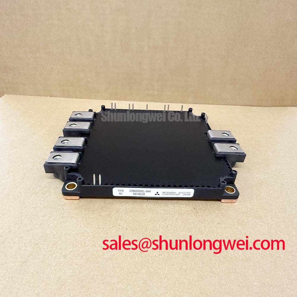
The Mitsubishi Electric CM600DXL-24S is an IGBT module with an official rated voltage of 1200.0 V, an official rated current of 600.0 A, and a Module package designation. These are the confirmed product-level specifications for initial purchasing, replacement screening, and cabinet-level compatibility review. The 1200 V rating does not by itself qualify the device for direct connection to a 1500 V DC bus; the inverter topology, switching transients, protection network, and operating margin must be assessed together.
| Parameter | CM600DXL-24S | Classification |
|---|---|---|
| Manufacturer | Mitsubishi Electric | Product identification |
| Rated voltage | 1200.0 V | Official specification |
| Rated current | 600.0 A | Official specification |
| Package | Module | Official physical classification |
For device identity and broader power semiconductor context, engineers can consult the Mitsubishi Electric power semiconductor resource. The product page for this part is available at CM600DXL-24S.
Gate disturbance during a high voltage transition should be investigated at the actual gate terminals, not inferred from the driver supply alone. A rapid collector voltage change can couple through device capacitances and the common gate return path, producing an unwanted gate excursion. In a half bridge, that excursion may increase the risk of cross conduction if the complementary device has not reached a secure off state.
Design Consideration: A low impedance active Miller clamp can provide a controlled discharge path during the interval when the opposing switch is turning on. If the selected driver supports negative gate bias, the system designer may evaluate a negative off-state level within the driver and module operating limits. Values such as a negative gate bias range are driver design choices, not official CM600DXL-24S ratings, and should not be treated as a guaranteed requirement for this module.
Use a differential probe suitable for the switching environment and measure directly between the gate and its corresponding emitter connection. A probe connected to a distant control ground can hide the real transient or create a measurement loop that exaggerates ringing. Compare the waveform during hard switching, regenerative braking, and abnormal load interruption. The useful observations are the peak gate excursion, ringing duration, turn-on delay consistency, and relationship between the disturbance and the complementary gate command.
Keep the power commutation loop physically separate from the gate driver loop. Minimize parasitic inductance in the gate return and avoid routing the gate trace beside a high dv/dt collector or DC bus conductor for long distances. If a gate spike remains after the driver clamp is enabled, inspect emitter reference movement, driver supply decoupling, isolation capacitance, and the physical location of the probe reference. The final switching waveform should be validated against the DC-link voltage, load current, and protection thresholds during controlled testing.
💡 Bench Tip: Discharge the DC link, use ESD protection, and record a cold-state diode and terminal baseline before comparing a replacement module with a known-good assembly.
Field Diagnostics & Commissioning: Evaluating Thermal Capacitance vs Heat Sink in CM600DXL-24S Topologies
Transient thermal behavior is governed by the complete path from semiconductor junction to case, interface material, heat sink, airflow system, and enclosure. A short overload pulse can be absorbed partly by the thermal capacitance of the module and surrounding structure, while repeated regenerative braking pulses can gradually raise the case and junction temperatures. The 600.0 A rating is an official product parameter, but it is not a universal operating current for every pulse width, switching frequency, cooling condition, or duty cycle.
For commissioning, log case temperature, coolant or air temperature where applicable, pulse duration, repetition rate, and current waveform as one data set. A multi-stage thermal model can then be fitted to the available transient thermal impedance information, with each RC stage representing a different heat-storage and heat-flow time constant. Peak junction temperature is evaluated by applying the measured power pulse to that model and adding the measured case reference temperature. This is an engineering calculation and requires the relevant thermal data and boundary conditions; it is not derived from the nominal current alone.
Regenerative braking choppers deserve particular attention because the brake resistor absorbs energy that may otherwise return to the DC link. The IGBT switching pattern, resistor pulse capability, bus capacitance, and braking threshold must be coordinated. When a braking event produces unexpected voltage overshoot, check the current decay path, busbar inductance, resistor connection, clamp network, and gate timing together rather than assigning the symptom to the module alone.
The freewheeling diode path also affects thermal stress and radiated emissions. Reverse recovery behavior depends on current, junction temperature, commutation speed, stray inductance, and the opposing switch. A softer recovery profile can reduce abrupt current change, but the appropriate result must be verified from the actual switching waveform. Snubber selection is a system engineering task: its placement should address the measured ringing loop, while its losses and temperature must be included in the thermal budget.
For a bidirectional battery DC to DC converter, alternating charge and discharge power can create repeated thermal cycles. Designers should monitor case temperature swing and dwell time between pulses, then compare the measured profile with the applicable module reliability and thermal limits. A thermal interface that is uneven, contaminated, or mechanically stressed can distort the result even when the electrical waveform appears acceptable. The thermal design and safe operating area discussion from Electronic Design provides useful general engineering context.
Transient Dynamics & Electrical Design: DC Bus Operating Voltage Headroom Derating on CM600DXL-24S
A 1200.0 V rated module requires careful separation between steady DC bus voltage and switching overshoot. In a utility-scale 1500 V high-power central photovoltaic inverter, the system designer must first establish whether the device is used behind a suitable conversion stage, within a lower-voltage sub-bus, or in another topology that keeps the device voltage within its validated electrical limits. Directly mapping a 1500 V system label to a 1200 V device rating would be an unsafe substitution assumption.
Voltage headroom is affected by busbar geometry, commutation inductance, current slew rate, snubber placement, gate resistance, diode recovery, and fault interruption. Capture the collector-emitter waveform at the module terminals during the highest expected current and fastest relevant transition. The measurement must include normal operation, regenerative events, startup abnormalities, and protective shutdown. Compare the highest measured transient with the applicable device limits and the system safety strategy.
Altitude and terrestrial neutron exposure may be relevant to high-voltage power conversion equipment installed above 2000 m, but a numerical SEB rate or FIT value cannot be assigned to this module without a qualified source and defined test conditions. Treat altitude, shielding, DC bus level, switching duty, and fault response as inputs to a reliability study rather than as a fixed product guarantee. The practical field action is to document site elevation, operating voltage, transient records, and protection response, then obtain a device-specific assessment where required.
For topology comparison, the CM450DX-24S1 can be reviewed as a lower current sibling product for an objective electrical and mechanical comparison; it is not an automatic replacement for the CM600DXL-24S. In the upstream rectification stage, engineers may also evaluate the CM100MXA-24S as a separate complementary device, subject to its own rating, pin arrangement, and thermal requirements.
Benchtop Waveform Tuning: Mitigating Stress via Common Mode Transient Immunity in Harsh Industrial Environments on CM600DXL-24S
Common-mode transient testing should begin at the isolation barrier and finish at the module gate-emitter waveform. A driver can experience a false command when the power-side reference moves rapidly relative to the control-side reference, even when the logic input appears clean. The investigation should cover isolation supply behavior, channel-to-channel timing, gate return inductance, shield or chassis coupling, and the physical clearance between power and control conductors.
Reinforced isolation, isolation withstand voltage above 5 kV, and CMTI above 100 kV/µs are system-level driver requirements that may be selected for a particular converter; they are not confirmed official specifications of the CM600DXL-24S. The module should be paired with a driver whose isolation rating, transient immunity, propagation delay, and output current are documented for the intended switching environment. Confirm these values from the selected driver documentation and test them with the module installed in the final mechanical arrangement.
During a controlled test, monitor both gate-emitter channels, the driver-side logic signals, isolated supply rails, and collector-emitter transitions. A false pulse may be associated with inadequate decoupling, isolation capacitance, an unstable gate return, probe coupling, or driver saturation. Check whether the event repeats at a particular bus voltage, current, temperature, or switching direction. Layout changes should preserve creepage and clearance, keep high-energy conductors away from control traces, and return gate current through the intended local path.
In troubleshooting work, the 1200 V CoolSiC™ MOSFET Advantage in Three Phase Power Conversion offers a useful comparison point for discussing high-speed switching, parasitic control, and system-level transient behavior. It should be used as technical context, not as evidence that the CM600DXL-24S has the same switching characteristics or driver requirements.