


Content last revised on September 27, 2026
CM600DY-24S Thermal-Electrical Optimization: Fault-Clearing Dynamics and Desaturation Protection
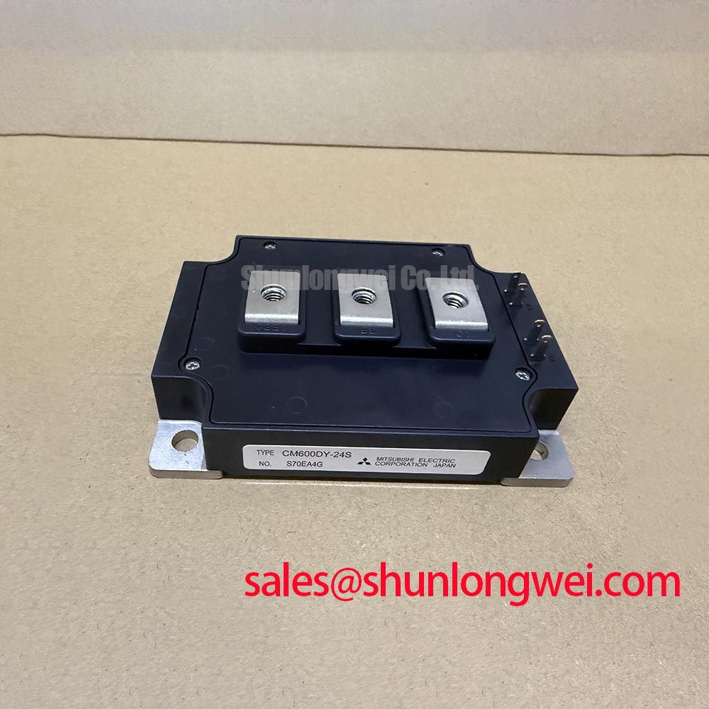
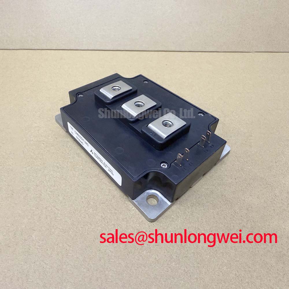
Begin the bench inspection by checking the nameplate against the required electrical boundary, then examine the module housing, terminal area, and mounting surface before applying any control or power voltage. The CM600DY-24S from Mitsubishi Electric is specified as a 1200.0 V, 600.0 A IGBT module in a module package. These are official product parameters supplied for identification; switching frequency, gate-drive conditions, short-circuit withstand capability, thermal impedance, internal circuit topology, and terminal assignment should be confirmed from the equipment documentation applicable to the installed unit.
For a utility-scale 1500 V high-power central solar photovoltaic inverter, system designers should not treat the module voltage rating as proof that the complete DC link is directly compatible. The inverter architecture, semiconductor series connection, switching transients, insulation coordination, protection thresholds, and operating derating must be reviewed together. A replacement assessment should compare the original bill of materials, gate-driver interface, mechanical envelope, busbar arrangement, cooling method, and protection logic rather than relying on voltage and current labels alone.
Before powering a replacement assembly, technicians should trace the gate-driver output from the isolated supply to the module terminals and confirm that the control reference, gate return path, and fault feedback wiring match the original inverter design. The CM600DY-24S product information supplied here confirms the voltage and current ratings, but it does not establish a manufacturer-approved desaturation delay, short-circuit safe operating area, or two-stage soft turn-off profile. Those values must come from the relevant Mitsubishi Electric documentation or the inverter manufacturer’s service data.
A practical protection review should examine whether the driver detects an abnormal collector-emitter condition quickly enough for the installed switching loop. A type-I response may be used by a system designer for rapid fault recognition, while a type-II response can provide a controlled turn-off sequence intended to limit the voltage rise caused by stray inductance. These descriptions are design concepts, not official CM600DY-24S timing specifications. The actual thresholds, blanking interval, fault latch behavior, and soft turn-off current profile require oscilloscope verification under controlled test conditions.
During troubleshooting, compare the gate-emitter waveform, collector-emitter voltage, desaturation signal, and driver fault output at the same time reference. An unexplained fault may involve gate-loop impedance, an incorrectly referenced isolation supply, excessive common-source or emitter-path inductance, optical or magnetic feedback delay, or a genuine power-stage event. A single alarm code should therefore be treated as a diagnostic starting point rather than proof of one failed component.
For photovoltaic inverter service work, the MOV network should be reviewed as part of the complete overvoltage path. An MOV may help absorb slower or externally induced surge energy, but it is not a substitute for a properly coordinated semiconductor clamp, snubber, DC-link capacitor network, and fast gate-drive protection. Designers should verify the MOV working voltage, energy rating, leakage behavior, thermal coordination, and failure-clearance method against the actual inverter bus and surge environment. The module’s 1200.0 V rating alone does not define the correct MOV selection.
The official Mitsubishi Electric Power Semiconductors and High-Power Modules resource should be consulted for manufacturer-level device information. A distributor product page can support part identification and sourcing decisions, but the final protection settings remain system-dependent.
CM600DY-24S Operational Boundaries: Isolated DC-DC Supply Evaluation
The isolated DC-DC supply for the gate driver should be assessed by tracing both steady-state behavior and transient response. The required output voltage, available gate charge current, insulation system, creepage and clearance, and fault behavior belong to the complete driver design. The supplied CM600DY-24S parameters do not specify a reinforced isolation rating or a common-mode transient immunity value for the gate-driver supply, so those figures must not be presented as guaranteed characteristics of this module.
When the inverter uses a high-voltage DC link, the isolation barrier should be evaluated against the equipment insulation coordination study and the relevant safety standard. Designers should verify whether the selected DC-DC converter and gate-driver interface can maintain signal integrity during the measured collector-emitter transition. If a false gate pulse appears during switching, inspect the isolation supply return path, driver reference connection, transformer or isolator layout, Miller coupling path, and local decoupling before assigning the fault to the IGBT module.
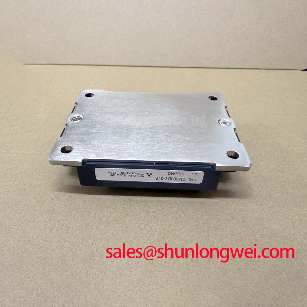
Thermal installation also deserves a physical inspection. The heatsink should be flat, clean, and free from burrs that could tilt the module base. Thermal interface material should be applied consistently according to the material supplier’s instructions; a thin, uniform layer is generally preferred, but the suitable thickness depends on surface flatness, material type, pressure, and the approved assembly process. The supplied product data does not define a universal 50 to 80 µm TIM requirement for this model.
Mounting pressure should be introduced progressively and evenly so that the baseplate is not locally distorted. A cross-pattern sequence is a common industry design consideration for multi-fastener power modules, while the final torque must be taken from the applicable mechanical drawing or installation documentation. ⚡ Safety Interlock Note: isolate and verify the DC link is discharged before disconnecting the gate-driver cable or touching the module terminals.
After assembly, verify insulation resistance and continuity using a test method suitable for the inverter’s insulation system. Do not infer the module’s internal construction or terminal arrangement from a visually similar package. The system integrator should verify every terminal function from the original module drawing and the equipment wiring documentation before applying a control signal.
Preventing Spurious Faults: Dynamic Power Loss and Multi-R Thermal Review
Thermal evaluation should begin with measured operating conditions rather than an assumed junction temperature. Record the DC-link voltage, phase current, switching pattern, ambient temperature, heatsink temperature, cooling airflow or coolant condition, and protection events. The CM600DY-24S is identified here as a 600.0 A module, but that rating does not by itself establish continuous current capability for a particular inverter, duty cycle, switching frequency, or heatsink assembly.
For pulsed overload analysis, engineers can use the manufacturer’s transient thermal impedance data together with the measured pulse profile. A multi-RC thermal model may then represent the short-duration junction-to-case response and the slower case-to-heatsink and heatsink-to-ambient paths. The resulting peak junction estimate should be compared with the official maximum ratings and the validated system derating policy. If the required thermal curves are unavailable, the correct engineering action is to obtain the applicable datasheet or perform a controlled thermal characterization rather than inventing a junction-temperature margin.
Dynamic losses should be separated into conduction and switching components during the review. Conduction behavior depends on current waveform and junction temperature, while switching loss depends on bus voltage, current, gate resistance, driver behavior, commutation path, and device temperature. The module rating label cannot substitute for the loss curves and test conditions required for a credible calculation.
In a bidirectional DC-DC battery interface, repeated charge and discharge operation can produce thermal cycling in the module, baseplate, interface material, busbar joints, and cooling assembly. A design consideration is to examine the complete temperature swing and dwell profile rather than evaluating only the highest instantaneous current. Engineers should correlate thermal measurements with fault logs and inspect mounting pressure, interface material condition, fan or pump performance, and busbar joints when intermittent faults occur. No field lifetime or failure-rate conclusion should be drawn without an authoritative test program or source document.
For comparative architecture work, the CM100DY-12E can be reviewed as a separate Mitsubishi Electric product reference, but its different voltage and current parameters mean that it should not be treated as a drop-in substitute without electrical, thermal, mechanical, and control-interface validation. Replacement selection remains the responsibility of the system engineer using the original equipment requirements.
CM600DY-24S Turn-Off Overshoot Control and Laminated Busbar Verification
During turn-off testing, place voltage and current probes so that the measurement loop does not add significant inductance or obscure the real collector-emitter overshoot. The physical principle is direct: unwanted commutation inductance interacts with the rate of current change and can raise the observed voltage above the DC-link value. The engineering objective is to minimize the high-current loop area, maintain symmetrical current paths, and verify the resulting peak voltage against the module’s rated boundary under the actual switching condition.
A laminated busbar can help reduce parasitic loop area when its positive and negative conductors are arranged with controlled spacing and a short commutation path. This is a layout principle, not a guaranteed CM600DY-24S construction requirement. The final geometry should be established from the inverter current path, mechanical insulation requirements, creepage and clearance, capacitor placement, and measured double-pulse or operating waveforms. The frequently cited target of less than 25 nH should not be assigned to this model unless it is explicitly required by the system design or supported by the applicable manufacturer documentation.
Snubber selection should follow measured ringing frequency, overshoot amplitude, pulse energy, capacitor technology, resistor pulse capability, and thermal dissipation. An RC or RCD network may address a particular switching-node behavior, while an MOV generally addresses a different surge-energy timescale. Combining these elements without coordination can increase losses or leave the critical transient unchanged. Designers should validate the network with differential voltage measurement, current measurement, thermal observation, and repeated switching tests at the intended operating boundary.
When a fault appears only during high-current turn-off, inspect the complete commutation path: DC-link capacitor terminals, laminated busbar joints, module terminal interfaces, gate-return routing, clamp placement, and probe technique. A high-voltage spike may indicate excessive parasitic inductance, an unsuitable gate-drive transition, measurement error, or an interaction between the clamp and the power-stage resonance. Verification against a known-good waveform and the approved Mitsubishi Electric application data is required before changing gate resistance or protection thresholds.
For broader technology context, engineers reviewing high-voltage switching architectures may consult The 1200 V CoolSiC™ MOSFET Advantage in Three. It describes a different semiconductor technology and should be used for technical comparison, not as evidence of CM600DY-24S electrical characteristics. Additional manufacturer information is available through Mitsubishi Electric Global Semiconductor Device Technologies.