

Content last revised on September 29, 2026
FF400R07KE4 Electrical Identity and Incoming Inspection
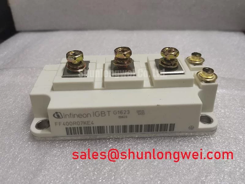
Begin the bench inspection by confirming the nameplate marking, checking the module body for mechanical damage, and measuring the cold state impedance between the relevant power terminals against a known good reference before applying any control signal. The FF400R07KE4 is an Infineon IGBT Module with an official rated voltage of 650 V and an official rated current of 400 A. Its package classification is Module. These three values identify the published product category and electrical rating; they do not by themselves define the permissible switching frequency, short circuit duration, thermal operating point, or complete inverter operating envelope.
For a utility scale centralized battery energy storage PCS, the module may be evaluated in the bidirectional power conversion stage where a controlled DC link is converted into grid side AC, or where grid energy is returned to the battery system. The system engineer should confirm the original converter topology, gate driver arrangement, cooling method, switching conditions, and protection coordination before treating this device as a service replacement. A nameplate match is not a substitute for verifying terminal topology, gate polarity, control timing, and the thermal interface used by the original assembly.
| Manufacturer | Infineon |
| Part number | FF400R07KE4 |
| Rated voltage | 650 V, Official Specification |
| Rated current | 400 A, Official Specification |
| Package | Module, Official Product Classification |
During incoming inspection, compare the power terminal condition, control terminal alignment, baseplate flatness, and mounting hole condition with the removed assembly. If the replacement is being assessed against another power module, the engineer should compare the full datasheet rather than relying on current and voltage labels alone. The FZ3600R12HP4 can be reviewed as a separate device during a neutral replacement study, but electrical, mechanical, thermal, and protection compatibility must be verified independently.
Preventing Spurious Faults: Baseplate Convexity Compensation and Screw Guidelines for FF400R07KE4
Clean both the module baseplate and the heatsink mounting surface with a method approved for the assembly, then inspect for burrs, embedded particles, and local surface damage. A power module depends on uniform pressure across its thermal contact area. Localized pressure can leave part of the baseplate poorly coupled to the heatsink while placing mechanical stress on the package. Baseplate curvature or convexity should therefore be measured with the same inspection method used for the original PCS service procedure, rather than corrected by excessive screw force.
Thermal interface material should be applied as a continuous, controlled layer that fills microscopic surface irregularities without creating thick pools or unfilled regions. The exact material and application thickness are system dependent. Designers should follow the thermal interface supplier’s process window and verify coverage after trial assembly. Voids, contamination, and trapped air can increase thermal resistance and may also create an uneven pressure pattern during operation.
Use the original mounting hardware where its condition and specification are confirmed. Tighten the fasteners in a cross pattern with a calibrated torque tool, allowing the baseplate to settle progressively instead of loading one corner first. The final torque value must come from the module or system assembly documentation, not from a generic assumption about package size. If a dish spring, spring washer, or pressure spreader is part of the original clamping arrangement, check its orientation, seating, and compression condition before reuse.
Bench Diagnostic: Never connect or remove the gate and auxiliary wiring while the DC link or control supply remains energized.
After mounting, inspect the edge of the interface for displaced compound and confirm that the module body is not being forced against an enclosure or busbar. A thermal camera during a controlled low energy test can help identify uneven heat spreading, but temperature observations should be compared with phase symmetry and measured electrical loading. A single warm region may require inspection of the interface, current sharing, busbar geometry, or gate timing rather than an immediate conclusion about module damage.
FF400R07KE4 Circuit Protection and Fault Clearing Dynamics
Desaturation protection should be treated as a coordinated gate driver function, not as an independently guaranteed feature of the FF400R07KE4. The driver measures the collector emitter voltage during conduction and initiates a fault response when the measured behavior exceeds its configured threshold. Type I or Type II desaturation terminology, detection delay, blanking time, and short circuit safe operating area must be confirmed from the selected driver documentation and the applicable Infineon data for the exact switching arrangement. The commonly discussed sub ten microsecond response target is a protection design objective unless explicitly documented for the complete circuit.
During a short circuit event, an immediate hard turn off can produce high inductive voltage overshoot. A staged soft turn off can reduce the rate of current collapse, but its timing, gate resistance, clamp behavior, and fault latch sequence must be validated on the actual power loop. The designer should minimize stray inductance in the commutation path and verify the peak collector emitter voltage with a properly rated differential probe. The result must be checked against the module’s published voltage boundary and the DC link conditions used by the PCS.
The gate driver should distinguish a genuine desaturation event from noise coupled through the measurement path. Short, direct sensing connections, suitable blanking control, and careful Kelvin referencing can improve measurement integrity. The fault signal path should be checked during normal switching, startup, shutdown, and controlled abnormal tests. If the driver reports intermittent faults, compare the desaturation waveform with the gate voltage, collector emitter voltage, and current probe signal on the same time base. This can reveal measurement ringing, timing interaction, or a real loss of controlled conduction without assigning a single cause in advance.
Thermal protection remains a separate task. The rated 650 V and 400 A values are official identification parameters, not a universal operating point for every PCS duty cycle. Designers should calculate conduction and switching losses from the actual current waveform, modulation pattern, junction temperature assumptions, and cooling conditions. Any surge or inrush event should be assessed against the relevant transient ratings in the complete manufacturer documentation, with recovery behavior verified before returning the converter to service.
For the rectifier or front end of a related power conversion chain, engineers may also review the FZ800R12KS4_B2 as a separate peripheral topology reference. It should not be treated as an automatic companion or substitute for the FF400R07KE4.
Assembly Integrity and Layout Architecture for High dv/dt Switching
High dv/dt switching can couple a transient into the opposite switch gate through the Miller capacitance, common emitter inductance, driver ground impedance, and nearby power conductors. The practical response is to keep the gate loop compact, separate high current commutation paths from sensitive control wiring, and use a driver architecture with an active Miller clamp when the complete application requires it. The clamp must be verified for its current capability, activation timing, and interaction with the normal turn on command.
A negative gate turn off bias can be considered where the selected driver, module documentation, insulation system, and control supply all support it. The correct value is system determined; it should not be copied from an unrelated IGBT family. Excessive negative bias can create its own reliability and driver stress concerns, while insufficient control of the gate can allow unwanted turn on during a fast opposite device transition. The design team should check the gate voltage directly at the module terminals, not only at the driver output connector.
For a centralized battery PCS, the busbar arrangement should preserve phase symmetry and limit the area of the high di/dt loop. The DC link capacitor connection, module power terminals, snubber location, and return path should be evaluated together. Clearance and creepage must be designed from the working voltage, pollution environment, insulation material, and applicable system standard. The module itself should not be described as independently certified for complete equipment EMC performance; the assembled converter requires its own conducted, radiated, and immunity evaluation.
Bootstrap supplies, when used by the selected gate driver, require their own review of capacitor ripple current, charging path, diode reverse recovery, low duty cycle behavior, and startup sequencing. The FF400R07KE4 product identity does not specify a universal bootstrap capacitor or diode arrangement. The system integrator should verify the required driver supply voltage from the original gate drive documentation and confirm that the bootstrap node remains within its limits across the full switching pattern.
For wider background on selecting power modules, checking commutation behavior, and structuring reliability tests, engineers can consult the Power Electronics Masterclass. It should be used as an engineering reference alongside the exact device and converter documentation.
FF400R07KE4 Thermal Electrical Optimization and Insulation Verification
Thermal and electrical validation should be performed together because junction temperature, switching loss, gate timing, and fault margin interact during real PCS operation. Confirm the heatsink interface, cooling flow or liquid path, sensor location, and phase current balance before increasing test power. The official 400 A rating does not establish a constant permissible current under every switching and thermal condition. The operating point must be derived from the actual duty cycle and verified by measurement.
Any reinforced galvanic isolation barrier belongs to the complete module, driver, mounting, and converter insulation system assessment. Do not treat a claimed withstand value or common mode transient immunity value as confirmed for this product unless it appears in the applicable manufacturer documentation. Isolation testing should follow the equipment safety procedure and use a test voltage, ramp, duration, and discharge method selected by the responsible compliance engineer. Control and power terminals should be protected from unintended test stress.
Common mode transient current can travel through isolation capacitance, heatsink structures, shield connections, and measurement equipment. During commissioning, monitor the gate to emitter waveform at the module pins while observing the opposite switch transition. If a false pulse appears, inspect probe grounding, driver return routing, clamp timing, isolation power supply behavior, and busbar coupling. The corrective action may involve layout, shielding, gate resistance, driver logic, or sequencing, so the waveform evidence should guide the change.
Before release to service, repeat the controlled switching test at the intended DC link condition and load range, then review turn off overshoot, gate plateau behavior, desaturation response, phase symmetry, and thermal rise. The Infineon IGBT Modules and Discretes portfolio provides the manufacturer’s broader product context, while the Infineon Intelligent Power Modules portfolio is relevant when comparing integrated driver architectures. Final acceptance remains dependent on the exact module documentation and the measured behavior of the repaired PCS.