

Content last revised on September 18, 2026
DD175N34K Specifications and Inspection
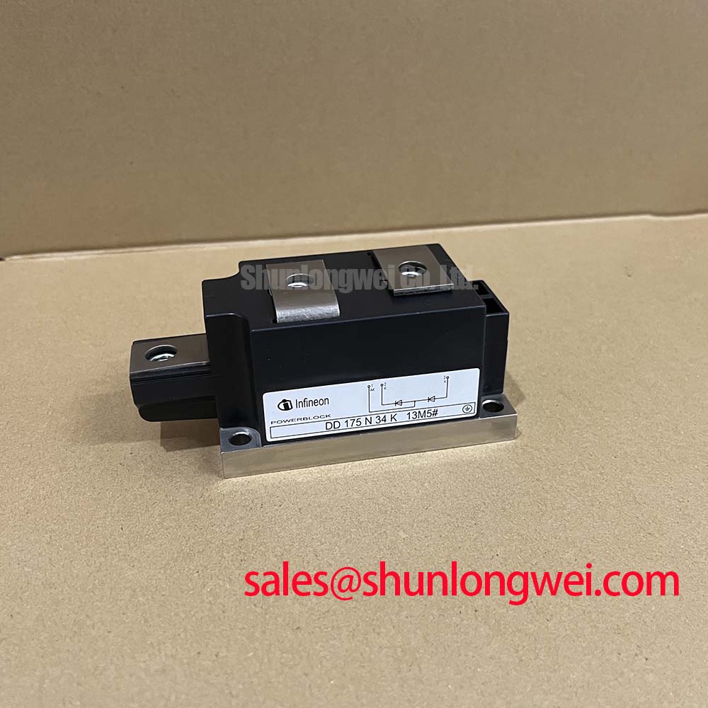
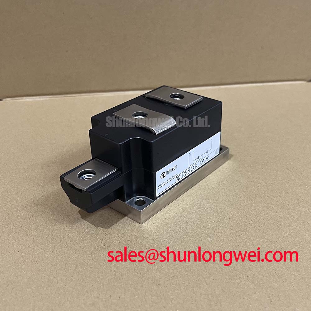
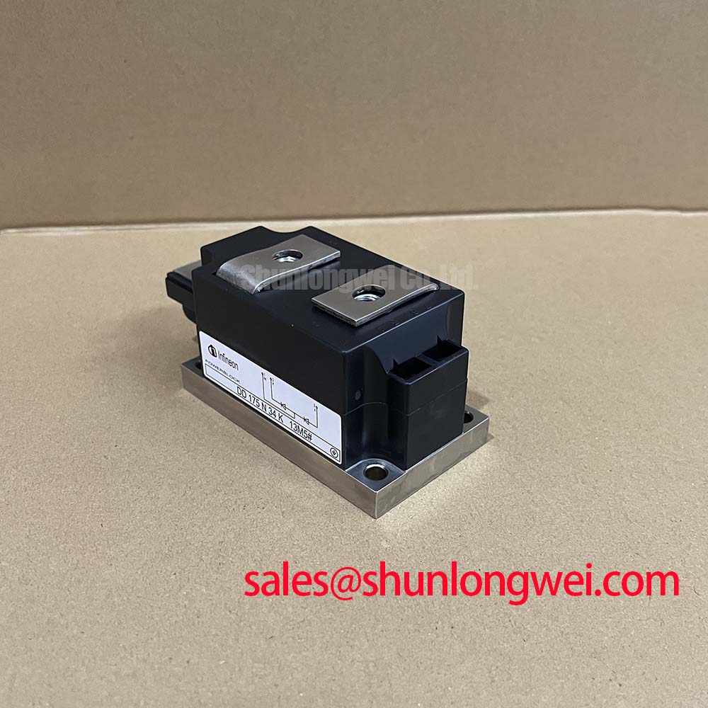
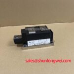
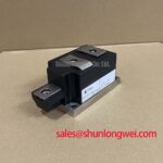
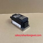
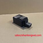
With the DD175N34K isolated from the power circuit, first confirm the terminal arrangement from the module markings and equipment documentation. If using a multimeter diode function, verify that its test voltage and current are suitable for this high-voltage power diode, and record the cold reading against a known serviceable assembly before reconnecting any busbar. This Infineon diode module is rated at 3400 V repetitive peak reverse voltage and 175 A average forward current at case temperature 100°C, making the specified electrical ratings the first check for replacement work in high voltage rectifier and commutation paths.
The official operating junction temperature range is minus 40°C to plus 150°C. Its specified isolation withstand is 3600 V RMS at 50 Hz for 1 minute. These are Official Datasheet Specifications and should be checked against the installed equipment’s voltage class, cooling arrangement, insulation test procedure, and circuit documentation. The DD175N34K is a diode module, so gate drive conditions, firing angle control, and unintended thyristor triggering belong to the surrounding controlled rectifier or soft starter system rather than to the diode itself.
| Official specification | DD175N34K value | Condition |
|---|---|---|
| Repetitive peak reverse voltage | 3400 V | VRRM |
| Average forward current | 175 A | IFAV, case temperature 100°C |
| Surge forward current | 4300 A | IFSM, 10 ms, junction temperature 25°C |
| Thermal resistance, junction to case | 0.11 K/W per diode | Rth(j-c) |
| Operating junction temperature | minus 40°C to plus 150°C | Tvj op |
| Isolation voltage | 3600 V RMS | 50 Hz, 1 minute |
| Mounting torque | 5 N·m ± 15% | Module mounting specification |
Assembly Integrity & Layout Architecture: Implementing Reverse Recovery Charge for DD175N34K
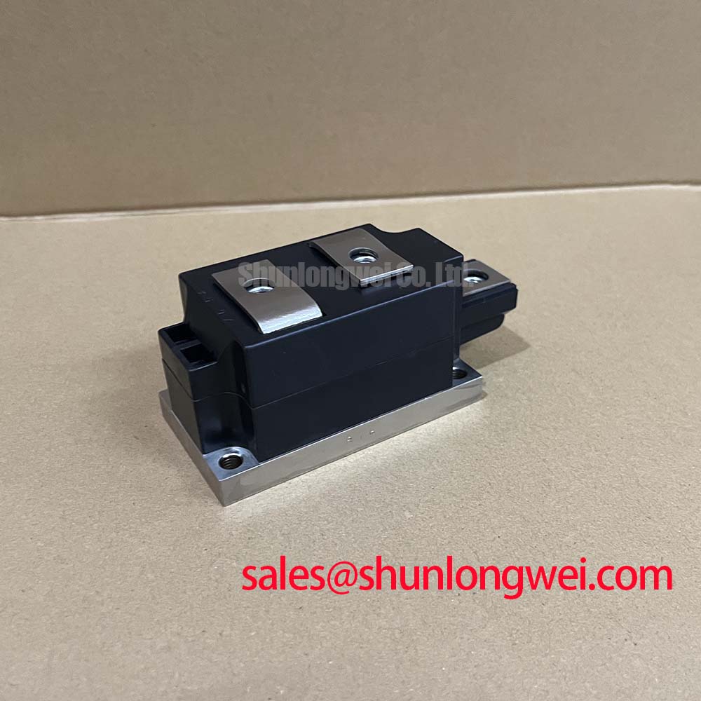
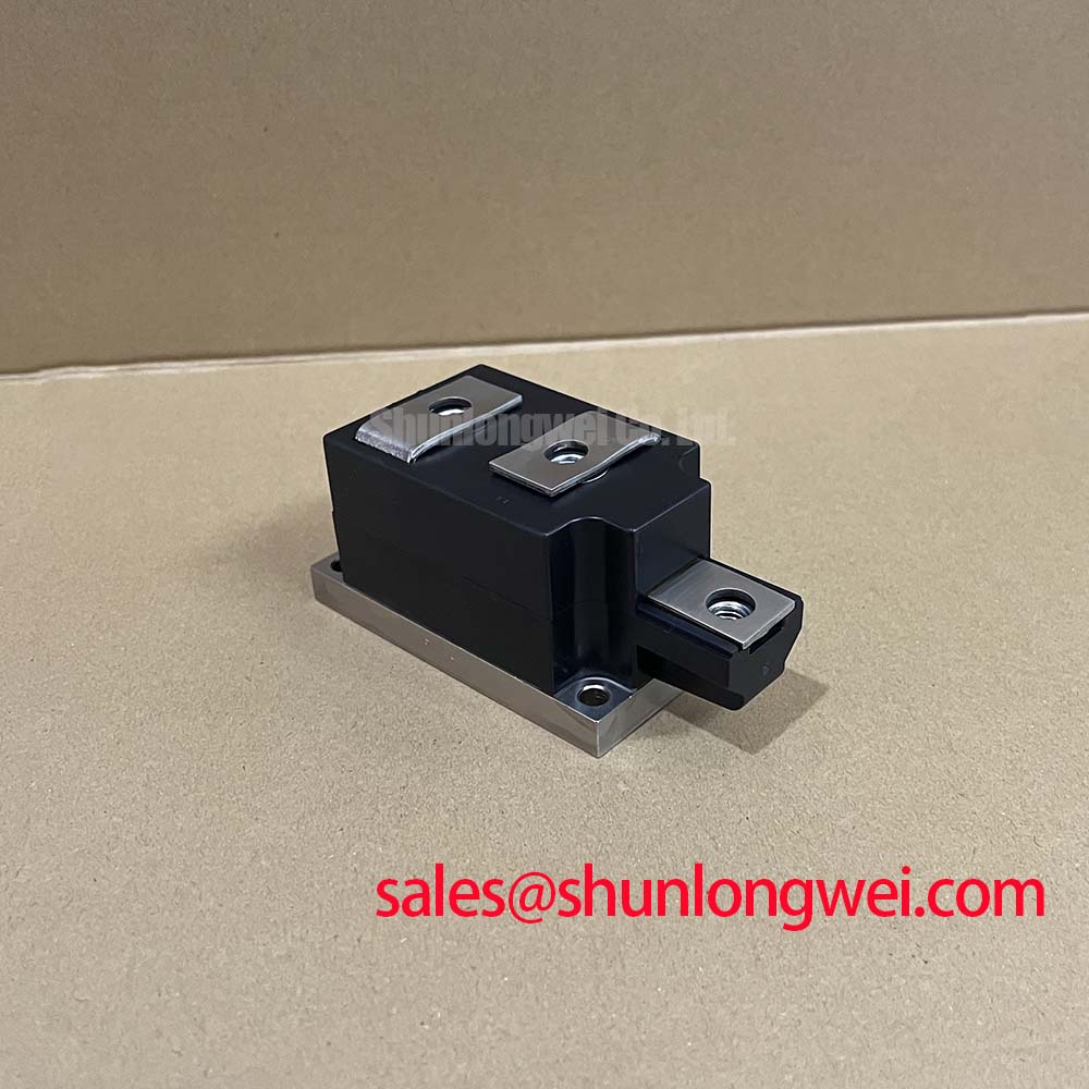
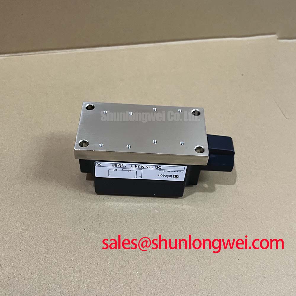
Before installing the DD175N34K, inspect the mating heatsink plane, terminal faces, mounting holes, washers, busbars, and cable lugs for flat contact and controlled alignment. A diode module can pass a static polarity check while the finished assembly still develops excessive commutation stress through loose hardware, oxidised conductors, or a long current loop. The module should be mounted with the official 5 N·m ± 15% torque requirement, using the original equipment’s approved mounting sequence so that pressure is distributed correctly across the baseplate.
🔧 Bench Diagnostic: Disconnect and discharge the DC link before loosening power terminals, then compare cold diode readings and insulation test practice with the equipment documentation rather than interpreting one meter result as a complete health verdict.
Reverse recovery current and reverse recovery time are important waveform variables in a commutating rectifier, but no Irrm, trr, reverse recovery charge, or softness specification has been provided for this DD175N34K data set. They should therefore not be assigned numerical values during repair planning. Engineering Recommendation: capture the actual commutation waveform with appropriately rated differential voltage and current measurement equipment after confirming safe test conditions. Compare the measured peak reverse voltage with the 3400 V VRRM boundary and investigate ringing, current overlap, or uneven phase behaviour through the full converter path.
Busbars should be arranged to minimize loop inductance where current transfers between the transformer secondary, semiconductor devices, DC link, and snubber components. This is a Design Consideration intended to reduce inductive overshoot during commutation; the acceptable layout is determined by system switching tests and verified peak margins. A metal oxide varistor can be part of a coordinated overvoltage absorption network when its voltage rating, energy capability, thermal environment, and upstream protection are verified by the system designer. It must not be assumed to replace a properly reviewed RC snubber or line filter.
Fuse coordination requires the fuse manufacturer’s time current curves, pre arcing and total clearing I²t information, and the protected circuit’s prospective fault current. The DD175N34K official surge rating of 4300 A for 10 ms at Tvj 25°C provides a defined surge condition, but it is not a substitute for a fuse I²t coordination table and should not be converted into an assumed clearing-energy limit. In assemblies that use controlled devices alongside this diode, inspect terminal allocation and connection drawings carefully; an incorrect anode or cathode connection changes the whole commutation path.
For a neutral comparison during a redesign review, the DDB6U180N16RRP_B37 can be examined against the original circuit’s voltage, current, thermal, terminal, isolation, and mechanical requirements. Matching a current label alone does not establish interchangeability.
Benchtop Waveform Tuning: Mitigating Stress via Harmonic Current Injection and Line Filter on DD175N34K
In a high voltage three phase motor solid state soft starter, the DD175N34K may be evaluated as part of a rectification or freewheel path only after the installed topology has been confirmed from the schematic. When firing angle is swept from 0 degrees toward 150 degrees in a phase controlled system, the AC to DC transfer characteristic, displacement power factor, harmonic current content, and reactive power demand can change materially. Those effects result from the complete converter, transformer impedance, motor condition, firing board timing, and line network. They are not individual factory ratings of the diode module.
A practical bench routine starts by recording line voltage, phase sequence, current waveform, DC link ripple, and heatsink temperature at controlled operating points. The aim is to identify whether one phase produces a different conduction interval, whether commutation overlap is changing, or whether the line filter is interacting with the controlled rectifier. A distorted current trace may indicate several conditions, including timing mismatch, supply imbalance, a degraded filter component, unequal branch impedance, or abnormal load behaviour. Use a known good signal path and system drawings to narrow the cause rather than assigning a single explanation from waveform shape alone.
Engineering Recommendation: evaluate line filter components, MOV protection, contactor condition, and transformer connections as a coordinated network. A filter may reduce conducted disturbance in an installed system, yet the diode module itself cannot be represented as independently compliant with equipment level EMC standards. The system engineer should verify conducted and radiated performance at the final equipment level under its intended operating modes.
Parallel diode branches also need careful interpretation. Equal static meter readings do not guarantee equal dynamic sharing, and no positive temperature coefficient characteristic is stated in the provided DD175N34K official data. Design Consideration: keep branch geometry, busbar resistance, thermal paths, and terminal contact conditions as symmetrical as practical, then validate current distribution under the actual waveform. The 0.11 K/W per diode junction to case thermal resistance is an Official Datasheet Specification useful for thermal assessment, but its use depends on the measured case temperature and the system’s loss calculation.
Where engineers need broader context on power semiconductor switching architectures, Infineon OptiMOS™ Low Voltage MOSFETs provides relevant manufacturer portfolio context. It does not establish characteristics for the DD175N34K diode module and should not be used to infer unlisted reverse recovery values.
DD175N34K Thermal Electrical Optimization: Short Circuit Withstand Limits: Coordinating Practical Tuning
A dead short event must be approached as a protection coordination problem, not as a claim that the DD175N34K can sustain a particular fault duration. The official data identifies 4300 A IFSM for 10 ms at 25°C junction temperature. That test condition is distinct from repetitive overload, elevated junction temperature, transformer-fed fault duty, or a fuse clearing sequence in a live soft starter. No short circuit withstand time, diode I²t limit, or repetitive surge endurance value is included in the stated official data, so such values should not be assumed.
During fault review, establish the available fault current at the module location, expected fuse operation, contactor opening behaviour, transformer contribution, and any stored energy in the DC link or snubber network. The protection team should compare the actual semiconductor fuse clearing characteristics with the converter’s expected fault current and all associated semiconductor ratings. This Engineering Recommendation helps prevent a repair decision from being based solely on the module’s surge current figure.
Thermal work should begin at the external interfaces. Remove old residue without scoring the contact surface, confirm heatsink flatness according to the equipment service standard, apply the specified thermal interface material consistently, and tighten the mounting hardware to the official torque requirement. A poor interface can raise case to heatsink temperature difference even when the cooling fan appears to operate normally. Thermal imaging, controlled load testing, and comparison with an equivalent healthy phase are more informative than estimating junction temperature from ambient air alone.
The stated minus 40°C to plus 150°C operating junction temperature range defines the module’s official operating boundary. It does not define a permitted recovery interval after an overload or an expected operating lifetime. After a surge or fault event, inspect the fuse, busbar joints, insulation barriers, heatsink interface, and all parallel paths before fitting a replacement module. Any insulation withstand test should respect the original equipment procedure and connected components that may be damaged by an inappropriate test voltage.
In systems using active switches elsewhere in the power stage, gate driver timing and fault response influence the stress applied to passive commutation paths. The Infineon Gate Driver ICs Portfolio is useful manufacturer context for reviewing driver functions in an associated converter. It does not mean that the DD175N34K includes a gate driver or requires a gate connection.
Assembly Integrity & Layout Architecture: Implementing RC Snubber Network Optimization to Prevent Stress for DD175N34K
An RC snubber should be reviewed as a circuit-specific damping network rather than fitted from a generic capacitor and resistor value. Its function can be to control voltage transient behaviour across a commutating device or branch, while a series saturable reactor may be considered where the system design requires control of current rise. The appropriate component values depend on measured ringing frequency, stray inductance, source impedance, current waveform, capacitor pulse capability, resistor pulse energy, temperature rise, and the converter’s operating sequence. The system engineer should verify the result on the assembled equipment against the 3400 V repetitive reverse-voltage specification.
For incoming inspection, check whether the existing snubber capacitor shows physical distress, whether the resistor has changed condition, and whether wiring has been moved away from its intended short connection path. A long return conductor can reduce the effectiveness of a correctly selected snubber because the added loop inductance participates in the transient. Do not assume that a MOV, RC snubber, and line filter are interchangeable protections. They address different parts of a system transient and disturbance problem and must be evaluated together.
The DD175N34K isolation rating of 3600 V RMS at 50 Hz for 1 minute is an Official Datasheet Specification for the module. Installation clearance, creepage, enclosure insulation, contamination level, cable insulation, and test method remain system responsibilities. Design Consideration: preserve the original insulating barriers and hardware arrangement, and verify that no busbar edge, loose washer, or displaced lead compromises the intended separation distance.
When troubleshooting recurrent commutation stress, check the measured AC supply waveform, firing synchronization, branch current balance, snubber condition, fastener torque, heatsink contact, and fuse coordination before attributing the issue to one component. For supporting background on three phase power conversion approaches, see The 1200 V CoolSiC™ MOSFET Advantage in Three. That technical reference concerns a different voltage class and device technology, so its values must not be transferred to the DD175N34K.