

Content last revised on October 6, 2026
EVM31-060 Thermal-Electrical Optimization: Optimizing Gate Drive Loop Geometry Before Practical Tuning
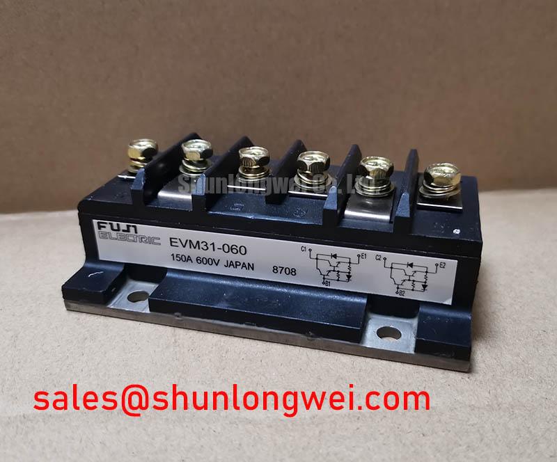
Begin at the installed gate-driver connector. Trace its gate and return conductors to the module terminals, then compare that route with the equipment schematic. A compact driver loop can reduce the voltage induced in the gate path during rapid current changes. If the original assembly provides a separate auxiliary emitter connection, route the driver return to that documented terminal rather than assuming a nearby power-emitter connection is equivalent. The available EVM31-060 product data does not establish its terminal assignment or confirm an auxiliary emitter terminal; verify both against the module drawing before changing the harness or circuit board.
Design Consideration: Keep high-current conductors from sharing a driver-return path where the verified terminal arrangement permits separation. Mutual coupling and shared return impedance can disturb the gate waveform, but oscillation should not be attributed to either cause without measurement. With suitable isolated instrumentation, compare gate-to-emitter waveforms at the driver and at the documented module terminals during controlled switching. Ringing that changes with current, wiring position, or the installed module can help narrow the investigation; the driver supply, probing arrangement, and external circuit still need checking.
Physical clearance matters when revising a driver board or harness, but no EVM31-060-specific clearance dimension is provided here. The system designer should set spacing from the equipment’s working voltage, insulation scheme, environment, and applicable assembly requirements. Do not treat the module’s 600 V rating (Official Specification) as a standalone rule for board spacing or DC-link operation.
For replacement assessment, 3MBI50SX-120-02 can be placed alongside EVM31-060 in a documented comparison, not treated as a confirmed drop-in substitute. Check the original drawings for terminal order, mounting interface, gate-drive requirements, thermal path, and each device’s applicable ratings before considering an electrical trial. Fuji Electric’s IGBT module product information provides broader manufacturer context, but a family overview cannot supply missing EVM31-060 pin or switching data.
EVM31-060 Thermal-Electrical Optimization: Four-Quadrant Power Flow Topologies for Practical Tuning
In a commercial string inverter or micro-grid storage system, engineers may evaluate this module within a bidirectional power stage that transfers energy between a battery-side circuit and a DC link. Four-quadrant operation describes the system’s controlled voltage and current directions; it is not an independently established capability of the EVM31-060 module. Confirm the equipment topology, the module’s switching role, and the current path in each operating mode before assigning it to charge or discharge service.
That distinction is useful during troubleshooting. A fault appearing only when power reverses may involve different freewheeling paths, driver commands, current sensing, or thermal loading. Capture the commanded gate states and measured current direction together, then compare them with the equipment schematic. For a stage containing other power modules, such as 6MBI15L-060, evaluate each device in its actual circuit position; a related part number alone does not establish a shared drive supply or compatible control sequence.
Design Consideration: Desaturation protection generally watches the conducting IGBT’s collector-to-emitter voltage for a rise inconsistent with its commanded on-state. It is not a fixed interpretation of a VCE(sat) figure detached from current and temperature. During a suspected short circuit, the driver must account for turn-on blanking, sensing delay, fault recognition, and the way gate charge is removed. A staged or soft turn-off may limit the resulting voltage overshoot, but neither a desaturation threshold nor a permissible detection time is established by the supplied EVM31-060 ratings. Confirm protection timing and short-circuit capability from the applicable device and driver documentation, then validate the assembled stage under controlled conditions.
Gate-trigger current and voltage specifications for a thyristor, and pulse-train firing practices associated with them, should not be transferred to this IGBT gate-drive evaluation. Likewise, a thyristor surge-current limit does not establish how this module withstands a short circuit or how long it must cool afterward. Those questions require the correct device documentation and a measured junction-temperature assessment, rather than an analogy between different switching devices.
EVM31-060 Operational Boundaries: Evaluating Dynamic Power Loss Dissipation and Multi-RC Limits
Start a pulsed-load assessment with the current and switching records from the actual converter, not its nominal power label. The 150 A current rating (Official Specification) does not, by itself, define allowable repetitive peak current, pulse duration, or case temperature. Conduction loss depends on the voltage across the device while carrying current; switching loss depends on the energy dissipated during transitions. The relevant values must be obtained for this module at applicable test conditions before a numerical loss estimate can be defended.
A multi-RC thermal model can represent how heat moves toward the case over different time scales, making it useful when battery charging, discharging, or peak shaving produces uneven loading. For EVM31-060, however, no transient thermal impedance curve or model coefficients are included in the supplied product data. Without them, a calculated peak junction temperature would imply precision the available specifications cannot support. Use the manufacturer’s applicable thermal data, measured case temperature, the equipment’s cooling conditions, and the recorded load profile to evaluate peak and repeated-cycle margins.
At the bench, inspect the mounting surface and compare the installed clamping method with the equipment service instructions. An uneven interface or changed cooling airflow can alter case temperature without any change in the electrical command. Record case temperature near the operating condition being investigated, then examine whether the current waveform, switching behavior, and cooling state changed at the same time. A hotter case does not identify a single failed component on its own.
⚠️ Field Alert: Isolate and discharge the DC link before disconnecting module terminals or gate-drive wiring.
Repeated thermal swings deserve attention in bidirectional storage equipment, but no operating-life figure or cycle limit can be assigned to EVM31-060 from the supplied ratings. Compare thermal measurements across the equipment’s actual charge and discharge duty, and use the module’s documented thermal limits when available. The discussion in The Advanced Thermal Management Revolution offers background on cooling approaches; it does not identify the internal construction or lifetime of this specific module.
EVM31-060 Operational Boundaries: Evaluating High dv/dt Cross-Conduction Shoot-Through Limits
When one switch in a converter leg changes voltage rapidly, current coupled through the opposing switch’s capacitances can disturb its off-state gate voltage. That mechanism is a reason to inspect gate-return impedance, off-state driver behavior, and switching-node waveforms when investigating suspected cross-conduction. It is not evidence that EVM31-060 requires a particular clamp circuit or negative gate voltage; those choices depend on documented gate limits, the driver, and measured system behavior.
💡 Pro Tip: Keep the power-loop layout balanced where practicable, then use controlled switching measurements to check turn-off overshoot against the documented device limit.
An active Miller clamp can provide a low-impedance off-state gate path in a compatible driver design. Before evaluating one, confirm the module terminal map and driver connection, and measure the off-state gate waveform at the correct reference point. Negative gate bias is another system-level option, but its value must remain within the device’s documented gate limits and be validated with the selected driver. Neither an active-clamp requirement nor an acceptable negative-bias setting follows from the 600 V and 150 A ratings alone.
If opposing gate signals appear to overlap, first check the commanded dead time against the waveforms measured at the module connections. Probe grounding and long measurement leads can make a fast transition look worse than it is; repeat the capture with an appropriate measurement arrangement before changing protection settings. Then examine driver supply stability and the power-loop layout while checking peak switching voltage against the module’s documented limits. Fuji Electric’s brake chopper IGBT module information illustrates another switching application, but its topology and device details should not be assumed to apply to EVM31-060.