
Content last revised on September 10, 2026
Benchtop Waveform Tuning: Mitigating Stress via High dv/dt Cross-Conduction Shoot-Through on FF600R12KF4
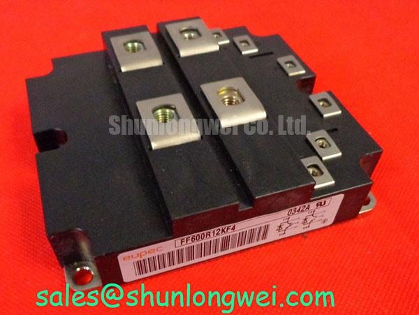
Begin a replacement inspection by recording the nameplate rating, checking the module housing and terminals for mechanical damage, and confirming the cold-state terminal resistance against the approved service procedure. The FF600R12KF4 is an Infineon IGBT Module with an official rated voltage of 1200.0 V and an official rated current of 600.0 A. Its package classification is Module. These values identify the device category and electrical rating, but they do not replace the complete manufacturer datasheet limits for switching conditions, temperature, gate drive, short-circuit operation, or thermal management.
| Parameter | Official Product Data | Engineering Interpretation |
|---|---|---|
| Manufacturer | Infineon | Confirm the original equipment documentation before integration |
| Model | FF600R12KF4 | Use the complete ordering designation during procurement and service work |
| Rated voltage | 1200.0 V | Verify switching overshoot and DC-link conditions during testing |
| Rated current | 600.0 A | Check current waveform, thermal conditions, duty cycle, and parallel-device balance |
| Package | Module | Confirm terminal arrangement, mounting interface, and cooling assembly compatibility |
The 1200 V and 600 A ratings are official specification data supplied for this product page. They should be treated as device identity and rating information rather than as permission to operate continuously at those limits in every converter topology. The system designer should verify the complete electrical and thermal operating envelope from the applicable Infineon documentation and the original equipment design.
High dv/dt testing should start with the gate and emitter waveforms measured at the module terminals, not only at the driver output. A fast collector voltage transition can couple through the device capacitances and raise the inactive switch gate voltage. If that gate excursion reaches the turn-on threshold while the opposite device is conducting, the resulting cross-conduction event can produce excessive current, local heating, or an apparent driver fault. The waveform must therefore be assessed at the power module, with the probe connection arranged to minimize measurement-loop inductance.
A low-impedance gate-drive path is a general design consideration for controlling this behavior. The power gate return and the auxiliary emitter reference should follow the intended driver topology without sharing unnecessary high-current commutation paths. An active Miller clamp can provide a controlled low-impedance path during the off-state, but its effectiveness depends on the driver architecture, clamp timing, gate resistance, common-emitter inductance, and the measured switching waveform. The clamp voltage and any negative gate bias are system decisions that require verification against the applicable Infineon gate-emitter limits; they are not universal FF600R12KF4 factory settings.
During bench tuning, compare the commanded gate signal with the actual gate-emitter voltage while observing collector-emitter voltage and phase-leg current on the same time base. A gate pulse that appears clean at the driver board may show ringing at the module because of the interconnect path. If a fault appears only at elevated switching speed, inspect driver isolation behavior, gate-loop routing, auxiliary emitter connection, dead-time coordination, and the physical distance between opposing power paths. A repeated fault should not be assigned to the IGBT alone until the known-good signal path and the complete commutation loop have been measured.
Short-circuit protection deserves separate attention. A desaturation circuit, soft turn-off strategy, and fault latch should be evaluated as a coordinated protection sequence. The soft turn-off profile must limit the energy released into the module and the DC-link commutation network while avoiding a new voltage overshoot. The required response time and gate discharge profile are determined by the system short-circuit test results and the complete device data. Designers should verify the protection sequence using controlled tests, current-limited laboratory equipment, and appropriate high-voltage safety procedures.
The charge associated with the Miller region and the collector-emitter transition varies with operating voltage and current. For this reason, a gate resistor selected from a low-voltage bench test may not provide the same behavior in the final converter. Cres-related coupling, driver output impedance, loop inductance, and temperature should be considered together. The Precision Gate Drive Design reference provides a useful system-level context for checking these interactions without treating a general design note as a product-specific guarantee.
Preventing Spurious Faults: DC-Link Capacitance Bank Layout and Low-ES Guidelines for FF600R12KF4
Inspect the DC-link assembly from the switching terminals outward. The local capacitor bank, laminated busbar, module terminals, snubber connection, and return path form one commutation network. Any unused length or asymmetry in this path can increase parasitic inductance and convert switching current slope into a collector-emitter voltage spike. In engineering terms, the peak voltage rises with the DC-link voltage and the product of commutation-loop inductance and current transition rate. This relationship should be used as a measurement principle, while the permitted peak margin must be established from the full device datasheet and converter test plan.
A low-ESR capacitor bank can reduce dynamic voltage disturbance, but capacitor selection alone cannot correct a poorly arranged busbar. Place the high-frequency commutation path close to the module power terminals and keep the forward and return conductors geometrically coupled. Symmetrical planar busbar geometry is a design consideration when several phase legs or paralleled modules share a DC link. The final arrangement should be verified with double-pulse testing, current-probe measurements, and high-bandwidth voltage probing at the module terminals.
When a replacement module is installed, verify the terminal identity against the original equipment drawing and the manufacturer documentation before applying power. Do not infer terminal polarity from physical position alone, particularly when the assembly uses laminated busbars, flexible links, or service adapters. Check creepage and clearance along the actual insulation surfaces, including spacers, fasteners, busbar edges, and contamination-prone areas. The required distances are system and working-voltage decisions governed by the applicable insulation design standard and enclosure conditions.
Mechanical stability also affects electrical behavior. Busbars should be supported so that vibration does not transfer repeated stress into the module terminals. Fastening hardware, insulating supports, and contact surfaces should be inspected for looseness, displacement, and uneven pressure during service. Mounting torque must come from the module documentation and the equipment assembly specification; a generic torque value should not be presented as an FF600R12KF4 factory requirement.
The Infineon EconoDUAL™ 3 product-family information can help engineers understand the intended industrial module context, but the applicable electrical, thermal, and mechanical limits remain specific to the exact part number and revision. Where the converter architecture uses a separate front-end or rectifier stage, engineers may also evaluate the associated FF45017ME4 page as a neutral reference for the surrounding power-conversion chain rather than as an automatic substitute.
FF600R12KF4 Circuit Protection & Reliability: Calibrating Gate Drive Loop Geometry
The auxiliary emitter connection should be routed as a control reference, not as an extension of the main high-current emitter conductor. Shared impedance between these paths can create mutual coupling during turn-off and produce a false gate signal at the driver input. The practical check is to measure the gate-emitter voltage directly at the module while the main emitter current changes. If the measured waveform differs substantially from the driver-board waveform, inspect the auxiliary return, connector contacts, copper overlap, and current path symmetry before changing the protection threshold.
Gate-loop geometry should minimize the area enclosed by the outgoing gate conductor and its return. Keep the driver connection physically consistent across parallel devices, and avoid routing sensitive control traces beside high-current collector or emitter conductors for unnecessary distances. The correct arrangement depends on the module terminal layout and the converter’s mechanical construction. It should be validated under the highest relevant switching stress, not only with a static continuity check.
Parallel operation requires both static and dynamic current sharing to be examined. Positive temperature coefficient behavior can support current balancing under suitable operating conditions, but it does not remove the need to match gate-drive timing, emitter-reference routing, thermal impedance, busbar geometry, and stray inductance. Engineers should compare the current waveform of each parallel path and check temperature distribution across the cooling interface. A current imbalance may originate in the driver, interconnect, thermal assembly, or measurement setup, so diagnosis should remain evidence-based.
Short-circuit protection should include a controlled desaturation or overcurrent detection strategy, an appropriate fault response, and a reset procedure that prevents repeated uncontrolled restart. Soft turn-off must be tuned with the power-loop inductance and clamp network in view. Excessively abrupt current interruption can increase voltage stress, while an overly slow response can increase short-circuit energy. The final balance is system-determined and must be demonstrated with the applicable short-circuit rating, test duration, junction-temperature condition, and DC-link state from the manufacturer’s documentation.
💡 Pro Tip: Keep the gate-drive return and auxiliary emitter reference physically separate from the main commutation-current route, then verify the result with simultaneous gate-voltage, collector-voltage, and current measurements.
For equipment sourcing, compare the original electrical rating, package interface, terminal arrangement, cooling method, driver compatibility, and protection sequence before considering another part. The FZ800R12KS4_B2 may be reviewed as a separate high-power module option, but compatibility must be established by the equipment designer rather than assumed from current or voltage figures alone.
FF600R12KF4 Circuit Protection & Reliability: Atmospheric Neutron and High-Altitude Assessment
Atmospheric radiation, altitude, insulation coordination, cooling performance, and electrical overstress should be handled as separate engineering questions. A specific FIT rate, Single Event Burnout probability, or operating-life value cannot be assigned to the FF600R12KF4 without an authoritative device-specific source, defined mission profile, voltage distribution, temperature history, and validated reliability model. The 1200.0 V rating is official product data, but it is not a radiation-reliability prediction.
For converters evaluated above typical low-altitude installations, the design team should review the change in atmospheric environment and then determine whether the application requires additional voltage derating, shielding analysis, monitoring, or qualification testing. Any claimed neutron-induced failure rate must be supported by a recognized reliability study, manufacturer qualification document, or applicable industry methodology. Without that source, the appropriate engineering action is to measure operating voltage, switching overshoot, junction-temperature indicators, and fault history rather than convert altitude into an unsupported failure percentage.
High-altitude equipment may also experience changes in cooling and insulation performance. Enclosure pressure, airflow, heat-sink capability, contamination, humidity, and partial-discharge risk should be evaluated according to the complete equipment design. Creepage and clearance must be checked for the actual working voltage, transient environment, pollution condition, and insulation material system. These are system-level compliance and reliability topics, not independent certifications provided by the IGBT module itself.
In a wind turbine full-scale converter, engineers may evaluate this module in a generator-side or grid-side power stage when the original topology, voltage class, current demand, cooling system, gate driver, and mechanical interface are compatible. Commissioning should include controlled DC-link energization, gate-signal verification, phase-leg dead-time checks, thermal observation, and switching tests at progressively higher operating conditions. The Infineon TRENCHSTOP™ IGBT7 technical discussion offers broader industry context, but it should not be used to infer unlisted construction details or reliability figures for this exact model.
When a field unit shows intermittent overcurrent, desaturation, or gate-driver faults, record the DC-link voltage, phase current, gate-emitter waveform, collector-emitter peak, cooling condition, and fault timing. Compare those measurements with a known-good phase leg and the original equipment limits. This process helps separate device stress from wiring, driver, capacitor-bank, thermal, and control-system causes before a replacement decision is made.