


Content last revised on September 23, 2026
FF600R12ME4P_B11 Circuit Protection & Reliability
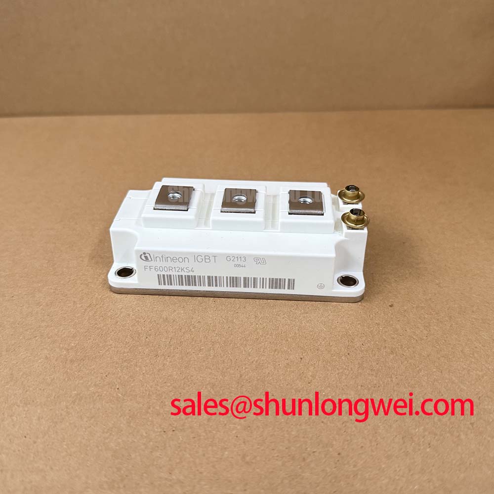
Before installation, verify the converter bill of materials, the module marking, and the DC bus design boundary against the official 1200 V collector-emitter rating of the FF600R12ME4P_B11. This Infineon IGBT module is specified for a 600 A rated DC collector current and 1200 A repetitive peak collector current under the applicable datasheet conditions, within the EconoDUAL 3 package using PressFIT control terminals.
| Technical Parameter | Official Specification |
|---|---|
| Collector-Emitter Voltage | 1200 V VCES |
| Rated DC Collector Current | 600 A IC |
| Repetitive Peak Collector Current | 1200 A ICRM |
| Collector-Emitter Saturation Voltage | 1.85 V typical at Tj = 125°C |
| Gate Threshold Voltage | 5.0 V to 6.5 V |
| IGBT Thermal Resistance with TIM | 0.0768 K/W RthJF |
| Package | EconoDUAL 3 |
| Control Connection | PressFIT pins |
| Temperature Monitoring | Integrated NTC thermistor |
The 1200 V VCES value is an official datasheet specification for the FF600R12ME4P_B11, not a declared operating DC link voltage. When this module is evaluated in a full-scale wind turbine converter, the system team should examine the measured DC bus excursion, switching overshoot, grid fault response, and protection reaction time as a combined voltage stress condition. These measurements matter because a nominal bus value alone does not define the electrical peak experienced at the IGBT terminals.
Atmospheric neutron exposure and possible single-event burnout are high-risk reliability subjects. No device-specific FIT rate, altitude derating curve, or guaranteed neutron withstand figure is stated in the supplied official specifications for this product. It would therefore be inappropriate to assign a failure rate or prescribe a fixed DC bus derating value for installations above 2000 m. Design Consideration: projects operating at elevation should treat altitude, site mission profile, converter topology, protection coordination, and measured voltage margin as system validation inputs rather than applying a generic percentage rule.
A practical review begins with recorded converter waveforms. Capture collector-emitter voltage during normal switching, regenerative events, fault interruption, and the worst expected grid transient. Compare the measured peak envelope with the module rating under the actual temperature and current conditions. Inspect the busbar geometry, DC link capacitor placement, snubber network condition, and the physical separation of high-energy conductors from gate drive wiring. A repetitive overshoot pattern can arise from several interacting causes, including increased commutation loop inductance, degraded capacitor connections, or altered gate drive behavior; it should be investigated with synchronized voltage and gate-source measurements.
The interaction between diode reverse-recovery behavior and conducted or radiated noise also deserves attention. The FF600R12ME4P_B11 product information provided here does not state a reverse-recovery softness factor, so no module-specific softness claim should be made. Engineering Recommendation: evaluate the commutation waveform on the completed converter, because reverse-recovery current shape, busbar inductance, gate resistance, and operating temperature together affect ringing and electromagnetic noise. Infineon’s TRENCHSTOP™ IGBT3 application material provides relevant context for switching behavior assessment.
For a higher-current reference in a separate converter architecture, engineers may compare electrical and mechanical documentation for the FZ3600R12HP4. Such a comparison is a documentation exercise, not a statement of interchangeability. Terminal arrangement, cooling interface, driver capability, protection thresholds, and inverter layout must be verified by the system integrator.
Assembly Integrity & Layout Architecture: Implementing Thermal Time Constants and Peak Junction Temperature for FF600R12ME4P_B11
The official thermal figure available for this module is RthJF = 0.0768 K/W for the IGBT with thermal interface material. This value supports thermal path assessment, but it does not by itself define the peak junction temperature during a pulsed overload. A switching converter produces time-varying conduction and switching losses, while the junction, baseplate, thermal interface material, heatsink, and coolant or airflow respond at different rates.
Design Consideration: use the manufacturer’s applicable transient thermal impedance information when available and combine it with the measured current waveform, switching energy data, duty cycle, heatsink performance, and ambient condition. A multi-RC thermal model can represent the delayed heat movement through the assembly, allowing the design team to estimate the junction rise associated with a defined pulse sequence. The final margin should be verified by system-level testing because mounting flatness, thermal interface quality, airflow distribution, and operating sequence influence the installed thermal path.
Switching frequency changes the balance between switching loss and cooling response. Rather than treating a frequency range as a universal derating table, evaluate the actual converter modulation, current spectrum, and cooling capability at each intended operating point. For a multi-megawatt wind turbine full-scale converter, this should include steady generation, low-speed operation, reactive power conditions, and transient load cases. The integrated NTC thermistor offers a local temperature signal for the converter control and protection architecture, but its interpretation should follow the system documentation and validated sensor placement assumptions.
Prepare the heatsink contact surface so it is clean, flat, and free from damage that would prevent uniform thermal contact. Apply the thermal interface material according to the material supplier and equipment documentation, then tighten the power terminals and mounting hardware with the sequence and torque specified for the assembly. ⚡ Safety Interlock Note: De-energize, discharge, and verify the DC link before touching module terminals or disconnecting control wiring.
After commissioning, compare NTC trends between similar converter legs under equivalent operating conditions. A temperature deviation does not establish one cause by itself; it can indicate unequal cooling, altered load sharing, interface degradation, or a sensing path concern. Inspect the cooling path and correlate temperature records with phase current and switching operating state before deciding on corrective action.
Field Diagnostics & Commissioning: Isolated DC-DC Power Supply Sizing for FF600R12ME4P_B11 Topologies
Before energizing the power stage, confirm continuity and seating of the PressFIT control terminals, then verify the gate driver output path against the module terminal map supplied for the converter. The official product information identifies PressFIT control pins but does not provide an approved isolated supply voltage, isolation barrier rating, common-mode transient immunity value, or gate driver power requirement. Those characteristics are properties of the selected driver and the completed converter, not published module ratings in the supplied data.
Engineering Recommendation: select and validate the isolated DC-DC supply as part of the gate drive subsystem. The review should include the gate driver’s required output current, gate charge behavior under the intended switching conditions, isolation coordination, startup behavior, desaturation or short-circuit protection architecture, and common-mode transient performance. Designers should verify that the chosen isolation barrier and driver immunity are appropriate for the measured switching environment rather than assuming a fixed reinforced isolation or CMTI value.
Commissioning should use controlled initial operation with protection logs active. Observe gate-source voltage at the device reference, collector-emitter voltage, phase current, and DC link voltage simultaneously. A gate pulse that appears correct at the driver output may differ at the module during a fast switching event if the return path shares inductance with power current. Uncommanded turn-on or irregular ringing may indicate several issues, including return-path coupling, driver supply disturbance, probe reference error, or a control timing problem. Verify the signal path against a known stable converter leg where available.
The Infineon RCDC application note can help frame commutation and reverse-conducting device behavior at a technology level. It should not be used to infer unpublished internal characteristics of the FF600R12ME4P_B11. For structured measurement practices and fault isolation workflow, consult the Field Engineer’s Handbook while retaining the original converter schematic and service documentation as the controlling references.
Assembly Integrity & Layout Architecture: Implementing Differential Gate-Source Loop Routing for FF600R12ME4P_B11
Route the gate drive as a compact differential gate-source loop and keep it physically distinct from the main collector and emitter current path. The aim is to reduce shared parasitic inductance, which can convert a fast-changing power current into an unwanted gate-source disturbance. This principle is particularly important where a high-current module is installed beside laminated busbars, capacitor banks, and multiple parallel drive channels.
The supplied specifications do not confirm a dedicated auxiliary emitter or Kelvin emitter terminal configuration for this exact model. Do not assume one from the package name or from another EconoDUAL device. The integrator should verify the original module drawing and inverter terminal designation before assigning a driver return connection. If the validated terminal documentation provides a suitable low-current source reference, route that reference independently from the main power return wherever the converter layout permits.
Keep the gate command and return conductors closely coupled, avoid long parallel exposure to collector or power emitter conductors, and maintain clear separation between measurement leads and switching nodes. These are Design Considerations intended to suppress turn-off overshoot, gate oscillation, and measurement ambiguity. Final placement should be tested on the assembled hardware by checking peak collector-emitter voltage, gate-source stability, and current waveform behavior across the intended operating envelope.
💡 Pro Tip: Use a symmetrical DC link and busbar layout where practical, then confirm switching margin with double-pulse testing on the completed power stage.