Content last revised on October 11, 2026
FP10R12W1T3 Identification and Replacement Screening
- Confirm the nameplate and service record identify FP10R12W1T3 from Infineon before removing the failed power assembly.
- Record cold terminal readings with the DC link fully isolated and discharged.
- Inspect the mounting surface, thermal interface, busbar alignment, and signs of moisture or contamination.
- Check the isolated gate driver circuit and its protection logic before applying DC power.
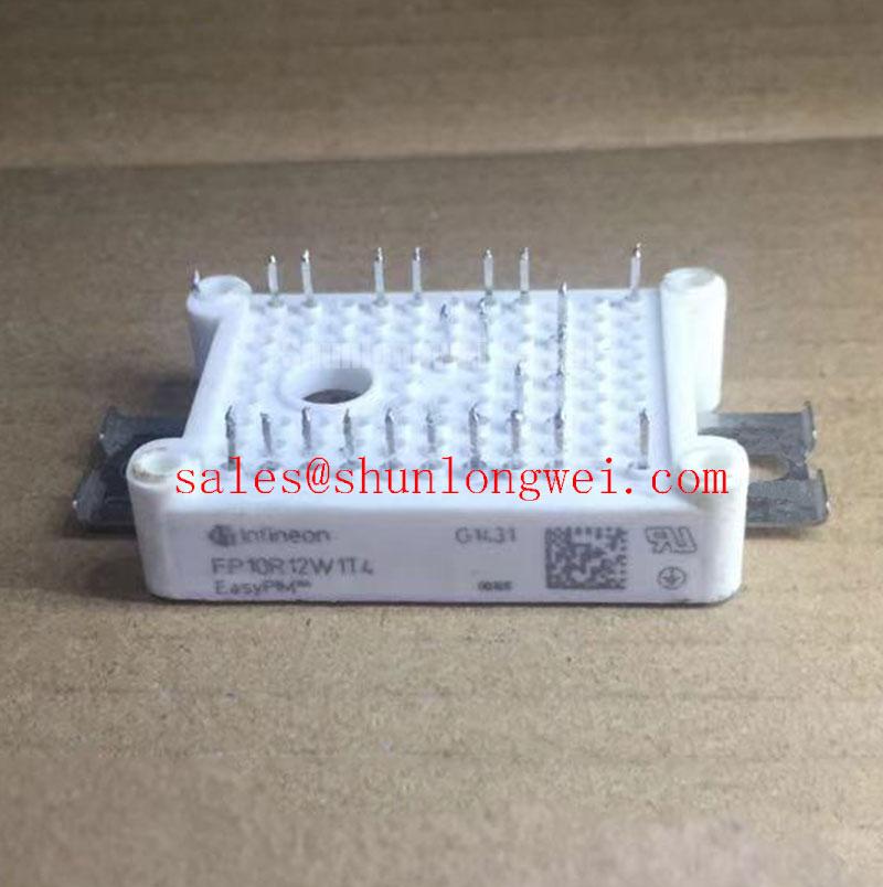
FP10R12W1T3 is an Infineon IGBT Module with a listed voltage rating of 1200.0 V and current rating of 10.0 A, in a module package. These are the available official product specifications for identification and replacement screening. Actual switching limits, gate requirements, thermal impedance curves, diode characteristics, terminal arrangement, and isolation ratings must be taken from the applicable manufacturer documentation for the exact production version.
| Parameter | Official specification |
|---|---|
| Manufacturer | Infineon |
| Part number | FP10R12W1T3 |
| Rated voltage | 1200.0 V |
| Rated current | 10.0 A |
| Package | Module |
For repair planning, this voltage and current class is commonly reviewed in motor inverter assemblies, compact variable frequency drives, and light industrial robotic articulator axes. Compatibility remains a system decision. The engineer should compare the original schematic, switching frequency, cooling arrangement, gate driver interface, protection timing, and mechanical footprint before authorizing a replacement.
FP10R12W1T3 Circuit Protection and Reliability: Calibrating Desaturation Detection
Desaturation protection belongs to the external gate driver and protection circuit; it should not be treated as an intrinsic protection function of the module. During commissioning, inspect the driver supply, gate return path, desaturation sense wiring, blanking network, fault latch, and soft turn off path as one protection chain.
A short circuit can drive the IGBT into a high current and high dissipation condition before the protection circuit reacts. The required response time is determined by the module’s short circuit safe operating capability, gate driver delay, blanking interval, bus voltage, stray inductance, and test conditions. If the equipment specification calls for type I or type II short circuit protection within a defined interval such as 10 µs, that interval must be validated against the applicable device data and the complete driver circuit rather than assumed from the part number.
Two stage turn off is a practical design consideration when a hard fault produces a rapidly changing collector voltage. The first stage reduces gate drive strength or current, allowing the driver to control the rate of current collapse. A second stage then completes turn off after the fault signal is securely latched. This approach can reduce the risk of excessive inductive overshoot, but the correct gate resistance, delay, and clamp behavior are system determined. Use a properly rated differential probe to observe collector emitter voltage, gate emitter voltage, fault timing, and the driver output during a controlled test.
Keep the desaturation sense conductor physically separate from high current commutation paths. Minimize the shared inductance between the driver return and the power emitter connection, and route the fault signal away from the switching node. Clearance around the high voltage terminals must suit the working voltage, pollution environment, insulation system, and enclosure geometry. A layout that appears adequate on a clean bench may behave differently when dust, condensation, or conductive contamination is present.
When a protection trip occurs, preserve the fault waveform before replacing the module. Inspect whether the fault signal arrives late, whether the gate voltage remains active after the fault latch, and whether the collector emitter overshoot approaches the available voltage margin. The switching loop, DC link capacitor position, busbar geometry, and clamp network should be reviewed together. Infineon’s technical material on IGBT discretes and co-pack diodes can provide useful background for interpreting switching and diode behavior, while the device specific limits remain controlling.
FP10R12W1T3 Circuit Protection and Reliability: Calibrating Unpowered Bench Screening with Multimeter Diode Testing
Cold screening should begin only after the inverter is isolated, locked out, and verified free of hazardous DC voltage. Use the equipment schematic or the original terminal marking to identify the collector, emitter, gate, and any auxiliary or diode terminals. Do not infer a pinout from a visually similar module.
With the module unpowered, use a digital multimeter in diode check mode to check the main semiconductor path in both polarities. With the gate uncharged, the IGBT direction should generally block while the antiparallel diode should conduct in its forward direction, if that diode is part of the verified module topology. Record the displayed values and compare them with a known serviceable unit. A single meter reading is not a pass or fail specification for this device. Differences between a known serviceable unit and the suspect unit are more useful, particularly when accompanied by gate leakage checks and a review of the external driver circuit.
For gate screening, connect the meter only according to the verified terminal map and avoid charging the gate with repeated uncontrolled probing. Gate leakage that differs materially from the reference assembly may justify removal from service, but the result should be correlated with contamination, moisture, meter polarity, and any connected snubber or driver components. Disconnect parallel circuitry when necessary so that the measurement represents the module rather than the surrounding board.
Bench inspection should also cover the mounting face, terminal plating, molded housing, fastener seats, and busbar interfaces. Look for uneven contact marks, loosened hardware, discoloration, mechanical stress, and deposits that could reduce creepage or create surface leakage. Creepage and clearance are installation properties as well as component properties, so the final assessment must include the barrier, busbar support, insulation sheets, and enclosure condition.
Vibration control is important in robotic articulator drives and other moving equipment. Busbars should be supported so that their mass does not load the module terminals, and fastening should follow the equipment manufacturer’s mechanical procedure. Thermal compound should be spread consistently across a clean, flat mating surface; excessive compound, a damaged insulator, or a tilted heatsink can increase thermal resistance even when the fasteners appear tight.
Maintenance Note: After recommissioning, trend terminal and heatsink temperature under a repeatable load and inspect the cooling path during scheduled cleaning rather than waiting for a protection trip.
For a neutral replacement comparison, engineers may review FP40R12KE3G against the original circuit, mechanical arrangement, electrical ratings, and gate drive requirements; it should not be treated as a drop in substitute without that comparison. In the rectifier and DC link portion of the same power chain, FP35R12KT4 may also be evaluated as an associated module, subject to the system schematic and operating conditions.
FP10R12W1T3 Circuit Protection and Reliability: Calibrating Common Mode Transient Immunity in Harsh Industrial Environments
Common mode transient behavior is governed by the complete isolated gate drive, mounting arrangement, switching loop, and control reference system. The 1200.0 V voltage rating of FP10R12W1T3 does not, by itself, establish a reinforced isolation rating or a common mode transient immunity value for the gate driver.
Where the equipment design requires reinforced galvanic isolation above 5 kV or a driver CMTI capability above 100 kV/µs, verify those figures from the selected driver’s safety documentation and test conditions. They should not be assigned to the IGBT module unless the exact manufacturer documentation states them. The test setup should reproduce the actual switching node movement, gate loop arrangement, isolation barrier, and fault monitoring connections.
Spurious gate pulses can result from capacitive displacement current, inadequate driver return control, excessive common emitter inductance, control cable coupling, or an improperly referenced probe. During troubleshooting, observe the gate emitter waveform at the module terminals rather than at the driver board alone. Compare the command signal, isolated driver output, gate voltage, and collector emitter transition on the same time base.
Keep isolated control traces away from the power commutation loop, maintain the required creepage and clearance for the working environment, and avoid routing signal returns across high di/dt current paths. The final spacing is determined by the insulation system, pollution degree, material group, altitude, and applicable safety standard. Any EMC result applies to the assembled equipment and its installation; the discrete module should not be represented as independently certified to CISPR or EN 55011.
For switching analysis, the reverse recovery behavior of the associated freewheel diode can influence voltage overshoot, ringing, and radiated emissions. Review the diode data, gate resistance, dead time, snubber arrangement, and busbar inductance as a coordinated network. The appropriate soft turn off profile and switching speed are established through controlled bench testing with voltage and current margins checked against the DC link conditions.
For additional background on semiconductor construction, switching stress, and protection principles, consult The Ultimate IGBT Knowledge Base. Infineon’s automotive qualified power module information is a separate reference category and should not be used to infer qualification status for this industrial module.