The Relentless Push for Power Density in Modern Electronics
In every corner of the power electronics industry, from electric vehicle (EV) chargers and solar inverters to industrial motor drives and data center power supplies, engineers face the same relentless pressure: deliver more power in less space. This isn’t just a trend; it’s a fundamental requirement. End-users demand smaller, lighter, and more efficient products. For the design engineer, this translates into a critical metric: power density (kW/L). The challenge is that simply shrinking a design often creates a new, more formidable problem—heat. Concentrating power generates immense thermal stress, which can compromise performance, reliability, and the lifespan of the entire system. This is where the often-underestimated science of IGBT packaging technology moves from a simple consideration to the absolute core of innovation.
For years, the focus was primarily on improving the silicon chip itself. While chip technology continues to advance, we’ve reached a point where the package—the housing that protects the silicon die, connects it to the circuit, and dissipates its heat—is no longer a passive component. It is the key enabler, or the primary bottleneck, in achieving the next leap in power density.
Decoding IGBT Packaging: More Than Just a Protective Shell
To the untrained eye, an IGBT module is just a plastic or ceramic block with terminals. But for an engineer, it’s a sophisticated electromechanical system designed to perform three critical functions simultaneously:
- Electrical Connection: The package provides low-resistance, low-inductance pathways from the silicon die to the external circuit (PCB or busbar). Poor electrical performance in the package, particularly high stray inductance, can cause voltage overshoots during high-speed switching, risking damage to the IGBT itself.
- Mechanical Stability and Isolation: It protects the fragile silicon die from mechanical shock, vibration, and environmental contaminants like moisture and dust. Crucially, it also provides the necessary electrical isolation between the high-voltage power circuit and the grounded heatsink, ensuring safety.
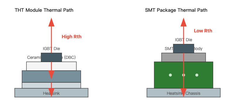
- Thermal Management: This is arguably the most critical function. The IGBT die can generate hundreds of watts of waste heat in a space smaller than a postage stamp. The package must create an efficient thermal bridge to transfer this heat away from the die and into a cooling system (typically a heatsink). Without this, the junction temperature would rise catastrophically in seconds.
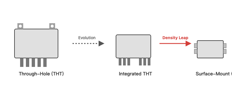
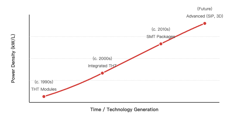
The evolution of packaging technology is a direct response to optimizing these three functions, leading us to the generational shift from through-hole mounting to surface mounting.
The Generational Leap: Through-Hole (THT) vs. Surface-Mount (SMT) Packages
The physical method of attaching an IGBT module to a PCB and heatsink has profound implications for its performance, manufacturing process, and ultimately, its power density. The two dominant approaches are Through-Hole Technology (THT) and Surface-Mount Technology (SMT).
Through-Hole Technology: The Established Workhorse
THT modules are the traditional stalwarts of the power electronics world. These packages, like the classic SEMIKRON SKM400GB12T4, feature screw terminals for high-current connections and solder pins that pass through holes in the printed circuit board (PCB). They are known for their robustness and ability to handle very high currents. The assembly process is manual or semi-automated, involving screwing the module to a heatsink and then soldering the control pins to the PCB. While reliable, this approach has inherent limitations in the modern era of automation and miniaturization.
Surface-Mount Technology: The Compact Innovator
SMT packages, as the name implies, are designed to be mounted directly onto the surface of a PCB. Instead of long pins and screw terminals, they use flat leads or solderable pads. This seemingly small change has revolutionary consequences. SMT assembly is fully automated using pick-and-place machines and reflow soldering ovens, drastically reducing manufacturing time and cost at scale. More importantly, the elimination of long leads and the potential for a more direct thermal path unlocks significant gains in both electrical and thermal performance.
Head-to-Head Comparison: THT vs. SMT
Understanding the trade-offs is crucial for any engineer or procurement manager. Here’s a direct comparison of the key characteristics:
| Characteristic | Through-Hole Technology (THT) | Surface-Mount Technology (SMT) |
|---|---|---|
| Assembly Process | Manual or semi-automated; requires separate screwing and soldering steps. Slower and more labor-intensive. | Fully automated pick-and-place and reflow soldering. Fast, repeatable, and cost-effective for high-volume production. |
| Size & Volume | Larger footprint and taller profile due to pins and screw terminals. | Significantly smaller and lower profile. Allows for double-sided PCB assembly, further increasing density. |
| Stray Inductance | Higher due to long internal bond wires and external screw terminals. Can lead to higher voltage overshoot. | Very low due to short, flat leads and optimized internal layout. Enables faster switching speeds and lower losses. |
| Thermal Path | Heat must travel from the die, through a ceramic substrate and a thick baseplate, to the heatsink. Higher thermal resistance (Rth). | Can offer more direct thermal paths. Some SMT packages are designed to be soldered directly to the PCB, which then dissipates heat through thermal vias. |
| Power Density | Lower. The physical size and less efficient thermal/electrical properties limit the power that can be handled per unit volume. | Significantly higher. The combination of smaller size, lower parasitics, and improved thermal potential allows for more powerful and compact systems. |
| Ideal Applications | High-power industrial drives, railway traction, utility-scale inverters, applications where manual assembly is acceptable. | Automotive onboard chargers, servo drives, compact solar micro-inverters, auxiliary power supplies, high-volume applications. |
For engineers struggling with design constraints, making the right package choice is critical. If your project demands high power but has space, a module like the Infineon FP75R12KT4 might be suitable. However, if space and automation are your top priorities, the SMT route is becoming unavoidable.
Case Study: Achieving a 40% Volume Reduction in a Servo Drive
Let’s translate this theory into a real-world engineering scenario.
The Challenge: A manufacturer of industrial robotics needs to design a new generation of compact servo drives. Their existing model uses a traditional THT IGBT module. The drive is reliable but bulky and requires significant heatsink volume, making it difficult to integrate into smaller robotic arms. The marketing team has mandated a 30% reduction in total volume without sacrificing performance.
The Solution: The engineering team decides to redesign the power stage around a modern SMT-based Intelligent Power Module (IPM). This module integrates the IGBTs, freewheeling diodes, and gate driver IC into a single, low-profile surface-mount package.
The Quantifiable Results:
- Volume Reduction: By eliminating the bulky THT module, screw terminals, and the need for a separate gate driver board, the total volume of the power stage was reduced by 40%, exceeding the target.
- Assembly Cost Reduction: The move to a fully automated SMT assembly line reduced the labor cost per unit by an estimated 25% and increased production throughput.
- Performance Boost: The low stray inductance of the SMT package allowed the team to slightly increase the switching frequency without excessive voltage overshoot. This enabled the use of smaller magnetics (inductors and transformers), contributing further to the size reduction and a 5% increase in overall efficiency.
This case study highlights that switching packaging technology is not just an incremental change; it’s a strategic decision that impacts the entire product architecture, from mechanical design to manufacturing logistics.
The Future is Flat: Emerging Trends in Power Module Packaging
The evolution doesn’t stop with SMT. The industry is pushing packaging limits even further, driven by the intense demands of applications like EVs and the advent of wide-bandgap (WBG) semiconductors like Silicon Carbide (SiC) and Gallium Nitride (GaN).
Double-Sided Cooling and Sintering
To extract every last watt of performance, future packages will be cooled from both the top and bottom. This technique, combined with replacing traditional thermal grease and solder with advanced silver sintering, dramatically lowers thermal resistance. Sintering creates a strong, thin, and highly conductive bond that can withstand much higher operating temperatures, a key requirement for SiC devices. To learn more, research shows sintering can improve thermal performance by over 20% compared to standard solder TIMs silver sintering for power electronics
The Rise of Embedded Die and System-in-Package (SiP)
Why mount a chip on a board when you can build the board around the chip? Embedded die technology involves placing the bare silicon die directly into the inner layers of the PCB itself. This creates the shortest possible electrical connections, virtually eliminating parasitic inductance and maximizing power density. This “System-in-Package” approach blurs the lines between component and system, leading to ultra-compact power converters.
How SiC and GaN are Forcing a Packaging Revolution
SiC and GaN devices can switch ten times faster and operate at higher temperatures than silicon IGBTs. This incredible performance is often wasted by traditional packaging. The high stray inductance of older THT packages acts like a speed bump, preventing these chips from reaching their full potential. Therefore, the adoption of SiC and GaN is a massive catalyst for the development of ultra-low inductance, high-thermal-performance SMT and advanced packages. You can explore this topic further in literature from leading power electronics research institutions IEEE transactions on power electronics packaging
Engineer’s Checklist: Selecting the Right IGBT Package
Choosing between THT and SMT isn’t always straightforward. Here’s a practical checklist to guide your decision:
- Power Level: For very high power ( > 50 kW), robust THT modules with screw terminals often remain the most practical choice due to their current handling capabilities. For low to medium power, SMT offers compelling advantages.
- Production Volume: Is this a low-volume, high-mix product or a high-volume, automated production run? The manufacturing cost benefits of SMT are most apparent at scale.
- Space Constraints: Is your design space-constrained? If so, SMT is the clear winner. The low profile and small footprint are unmatched.
- Switching Frequency: Are you operating at high switching frequencies ( > 20 kHz)? The low inductance of SMT packages is critical to minimize switching losses and EMI.
- Thermal Design: What is your cooling strategy? If you are using a traditional chassis-mounted heatsink, THT is straightforward. If you are exploring advanced cooling like PCB-based heatsinking, SMT is designed for it.
- Supply Chain and Sourcing: Do you have access to a reliable supply of both types of components? Working with a trusted supplier who offers a wide portfolio of both THT and SMT modules is essential. Need help navigating the options? Our expert team can provide guidance based on your specific application needs.
Conclusion: Why Your Next Big Innovation Might Be in the Package
The journey from bulky through-hole modules to sleek surface-mount packages is more than just a story of miniaturization. It’s a fundamental enabler of the efficiency, performance, and cost-effectiveness demanded by today’s most advanced applications. As silicon chips approach their theoretical limits, the package has become the new frontier for innovation in power electronics. Understanding the intricate trade-offs between different packaging technologies is no longer a niche skill—it’s essential for any engineer or product manager aiming to build a competitive, next-generation product.
The message is clear: to increase power density, you have to think inside the box. The right packaging choice will not only shrink your design but also unlock performance you never thought possible.